CANDE WORKSHOP 2008

Program     Location and Facilities

CANDE is the Computer Aided Network Design Technical Committee co-sponsored by CEDA (IEEE Council on Design Automation) and CASS (IEEE Circuits and Systems Society). It is a technical committee of both organizations with representatives on both the ICCAD and DAC executive committees. CANDE is dedicated to bringing design automation professionals together to assist in building relationships, furthering education and professional development as well as sponsoring initiatives that improve the EDA industry. CANDE sponsors a yearly workshop to address emerging technologies and the changing issues specific to the design, tools and academic communities. The workshop is organized to promote open discussion among the participants -- drawn from academia and industry. No proceedings are published and no recordings of the sessions are allowed. Time is provided in the program for full discussions (often quite lively) of the topics. The workshop attendance is intentionally limited to 40-50 so that everyone can participate in the discussions.

Each CANDE sesson involves presentations led by the speakers followed by a firing line at the end in which questions for all the speakers can be discussed.  Controversial topics and positions are especially encouraged as are candid answers from the experts. Particularly appropriate topics for CANDE include nascent ideas which might benefit from the substantive expertise of the CANDE members, negative technical results not suited for publication but which might well be instructive and long-range ideas which might not fit well at DAC, ICCAD or other EDA conferences.


Preliminary Workshop Program, CANDE 2008


Location and Facilities

Aerial view of hotel The CANDE workshop is an inclusive event, so registration includes lodging, all food, drinks and, of course, the technical program. Locations for CANDE are chosen to allow leisurely discussions between sessions in locales suited to relaxing walks, hikes or bicycle jaunts, again to encourage productive contact between workshop participants.  Speakers are a key part of the workshop and are usually available for detailed discussions in both public and private venues.

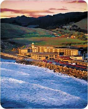
This year, CANDE will be held the evening of Thursday, Nov. 6 through Saturday, Nov, 8 ending in the early afternoon to allow return travel on the weekend. The location is the Lighthouse Hotel in Pacifica, CA. While a locally rural setting with a small artist town adjacent to the site, it is are short trip (18 miles) to San Francisco International Airport and allows easy access to the greater Bay area. As always, registrations are for the full conference, a special discount registration (not including additional lodging) is available for spouses or non-participating guests. Pacifica is a clement sea-side community with temperature averages between 10-18C (50-65F) with a small chance of rain in November. There are numerous walking and biking trails adjacent to the hotel as well as shopping and of course beach access within close walking distance. The Hotel Web site is:
https://www.bestwesternlighthouse.com/ and the Google Map URL is:
https://maps.google.com/maps?cid=0,0,14996598030813402332


BIOGRAPHIES:

  Steve Trimberger

Steve Trimberger received his PhD from Caltech at the dawn of the VLSI era, working with Carver Mead and Ivan Sutherland at Caltech, and Lynn Conway and Doug Fairbairn at Xerox PARC. Dr. Trimberger was a member of the original Design Technology group at VLSI Technology and joined Xilinx in 1988.

At Xilinx, Dr. Trimberger was a member of the architecture definition group for the Xilinx XC4000 FPGA and the technical leader for the XC4000 design automation software. He led the architecture definition group for the Xilinx XC4000X device families. He managed the Xilinx Advanced Development group for many years and is currently Distinguished Engineer in Xilinx Research Labs in San Jose where he leads the Circuits and Architectures Group. His research interests include low-power FPGAs, novel uses of reconfiguration, and cryptography.

Dr. Trimberger has written three books and dozens of papers on design automation and FPGA architectures. He is an inventor on more than one hundred patents in the fields of integrated circuit design, FPGA and ASIC architecture, CAE and cryptography. He has served as Design Methods Chair for the Design Automation Conference, Program Chair and General Chair for the ACM/SIGDA FPGA Symposium and on the technical programs of numerous Workshops and Symposia.


From Finance to Flip Flops: Using the Mathematics of Money and Risk to Model the Statistics of Nanoscale Circuits

Life gets interesting down in the nanometer regime. Devices with atomic dimensions don't have deterministic parameters: every behavior we want to model is a messy smear of probability. How should we attack such problems? Is slow, expensive Monte Carlo analysis our only option? Is the silicon community unique in facing such problems? As it turns out, problems in computational finance and risk analysis share many of the characteristics that challenge us in statistical circuit analysis: high dimensionality, profound nonlinearity, stringent accuracy requirements, and expensive analysis (i.e., circuit simulation). In this talk I'll show examples of adapting computational ideas from Wall Street for use in the silicon world. I'll show how the same methods used to price complex securities can be adapted to compute silicon yields, giving speedups of 2x - 50x. I'll show how methods used to analyze the statistics of rare events (like the size of the biggest wave in a hurricane like Katrina) can be used to analyze failures in SRAM, giving speedups of 20,000x. Some of our best engineering students have found careers on Wall Street in recent years. Work such as this suggests that this "brain drain" need not be such a one-way thing.

Rob Rutenbar

Rob A. Rutenbar received the Ph.D. from the University of Michigan in 1984, and then joined the faculty at Carnegie Mellon University. He currently holds the Stephen Jatras (E'47) Chair in Electrical and Computer Engineering. He has worked on tools for custom circuit synthesis and optimization for over 20 years.

In 1998 he co-founded Neolinear Inc. to commercialize the first practical synthesis tools for analog designs. He served as Neolinear's Chief Scientist until its acquisition by Cadence in 2004. He is the founding Director of the US national Focus Research Center for Circuits and System Solutions -- called "C2S2". C2S2 is a CMU-led consortium of 17 US universities and over 50 faculty funded by the US semiconductor industry and US government to address future circuit challenges.

He has won many awards over his career, including the 2001 Semiconductor Research Corporation Aristotle Award for excellence in education, and most recently, the 2007 IEEE Circuits & Systems Industrial Pioneer Award. His work has been featured in venues ranging from "EE Times" to "The Economist" magazine. He is a Fellow of the IEEE.


CEDA Technical Activities

The technical activity sub-committee of CEDA covers the activities where the implementation requires significant technical work.  These activities include planning for accreditation for new college programs (particularly international), a series of videotaped lectures available on the web (derived from the best papers of conferences and journals), and DUDE, a system that helps conference organizers find duplicate and/or potentially plagiarised submissions.

Lou Scheffer

Lou Scheffer received the B.S. and M.S. degrees from the California Institute of Technology, Pasadena, CA, in 1974 and 1975, respectively, and the Ph.D. degree from Stanford University, Stanford, CA, in 1984.

He worked at Hewlett Packard, from 1975 to 1981, as a chip designer and Computer-Aided Design (CAD) tool developer. In 1981, he joined Valid Logic Systems, where he did hardware design, developed a schematic editor, and built an IC layout, routing, and verification system. In 1991, Valid merged with Cadence Design System, San Jose, CA and, since then, he has been working on place and route and floorplanning systems. His research interests include physical design, particularly deep submicrometer effects. He enjoys teaching and has taught courses on CAD for electronics at the University of California, Berkeley, and Stanford University, as well as many tutorials for conferences and industry. He is also interested in Search for Extraterrestrial Intelligence (SETI), where he is the author of several papers, coeditor of the book, SETI 2020 (Mountain View, CA: SETI Press, 2003), and serves on the technical advisory board for the Allen Telescope Array at the SETI Institute.  Lou is currently working at Howard Hughes Medical Institute, seeing if IC design and reverse engineering tools can be helpful in the understanding of the brain's circuitry and wiring.


Efficient Programmable Processors and the End of ASICs

Today, most high-performance embedded applications are implemented by ASICs or ASSPs because their energy efficiency is 50-100x that of the most efficient programmable processors.  Designing an ASIC, however, costs $20M and two years, and this cost is increasing as applications become more complex.  This high cost limits ASICs to the highest volume applications and slows innovation.

The Stanford ELM processor optimizes data and instruction supply to realize a fully-programmable processor that is 30x more efficient than the best RISC processors and DSPs, and within a factor of 2-3x of hard-wired logic.   We expect the availability of such low-power processors to change the nature of embedded application development from ASIC design to real-time software development.

Bill Dally

Bill Dally is the Willard R. and Inez Kerr Bell Professor of Computer Science and Electrical Engineering and Chairman of the Computer Science Department at Stanford University. He is a member of the Computer Systems Laboratory, leads the Concurrent VLSI Architecture Group, and teaches courses on Computer Architecture, Computer Design, and VLSI Design. He is a Fellow of the American Academy of Arts & Sciences , a Fellow of the IEEE, a Fellow of the ACM, received the ACM Maurice Wilkes Award in 2000, and the IEEE Seymour Cray Award in 2004. Before joining to Stanford, Bill was a Professor in the department of Electrical Engineering and Computer Science at MIT .

Post-silicon validation - challenges and directions

Processor design trends and semiconductor technology scaling is making post-silicon validation an increasingly complex task. A new processor and chip-set can take between 1 and 2 years for validation from first tape-out before it can be shipped to customers. Improving post-silicon validation techniques is critical to shipping robust systems to customers and to reduce the time-to-market, which translates to competitiveness in the marketplace.

This talk gives an overview of post-silicon validation methodology used at Sun Microsystems. Trends which are making this task difficult are discussed.  Examples of some validation scenarios are described along with insight into the types of bugs that are typically found after silicon is available. Future challenges are discussed and some research directions that will help the industry in this area are proposed.


Ishwar Parulkar
      Ishwar Parulkar is a Distinguished Engineer at Sun Microsystems. His primary responsibility there is architecture, strategy and tools for DFX (Design for Testability, Diagnosability, Manufacturability, Yield), RAS (Reliability, Availability and Serviceability) and post-silicon validation. In this capacity, he works across the full spectrum from microprocessors, ASICs and servers to firmware and OS layers. In his 10 years at Sun, he has contributed to the quality, reliability and time-to-market of several successful products.

Ishwar received his M.S degree in Electrical Engineering from Vanderbilt University and he holds a Ph.D from the University of Southern California.  Prior to Sun, Ishwar worked at Apple, Inc. He has over 20 patents issued and pending.


Verification-Guided Error Resilience

Verification-guided error resilience (VGER) is the use of algorithmic verification, such as model checking, against a formal specification, to estimate a system's vulnerability to faults in devices and to reduce overheads of fault-tolerant design techniques. I will discuss our experience in applying VGER to dealing with soft errors in sequential circuits; for instance, on one design, our approach proved that the circuit was resilient to soft errors in latches while reducing the power overhead by about 80%. I will also briefly describe the connections between VGER and mutation-based techniques for evaluating the coverage of a design by a formal specification.

Sanjit A. Seshia

Sanjit A. Seshia is an assistant professor in the Department of Electrical Engineering and Computer Sciences at the University of California, Berkeley. He received an M.S. and a Ph.D. in Computer Science from Carnegie Mellon University, and a B.Tech. in Computer Science and Engineering from the Indian Institute of Technology, Bombay. His research interests are in dependable computing and computational logic, with a current focus on applying automated formal methods to problems in computer security, electronic design automation, and program analysis. He has received an Alfred P. Sloan Research Fellowship (2008), an NSF CAREER award (2007), and the School of Computer Science Distinguished Dissertation Award at Carnegie Mellon University (2005).


Statistical Variability and Reliability in Nano CMOS and Impact on Design

Statistical variability introduced by discreteness of charge and granularity of matter has become a major challenge for scaling and integration. It approaches more than 50% of the total variability in the 45 nm technology generation and with the introduction of restricted design rules (RDR) it is becoming the dominant component of the variability at the 32 nm technology generation. The statistical variability already profoundly affects SRAM design. In logic circuits it causes statistical timing problems and increasingly leads to hard digital faults. In both cases the statistical variability restricts the supply voltage scaling, adding to the power dissipation problems. In addition discrete trapped or permanent charges associated with different degradation processes, in combination with other sources of statistical variability, could result in rare but exceptionally large changes in the device parameters, as illustrated in Fig. 1 - 3 and in acute statistical reliability problems. This is already a fundamental problem in flash memories.

We will present simulation results illustrating the current status and the future trends in statistical variability. This will also include the distribution of threshold voltage and current changes due to the statistical trapping of degradation related discrete charges in random positions of the device in the individual and combined presence of other variability sources. The corresponding changes in the transistor characteristics are also captured in compact models which allow the study the impact of statistical reliability on yield during the life time of an integrated circuit. We will discuss also the impact of the statistical variability and reliability on design. The results are obtained in the framework of large national and collaboration project in Europe including NanoCMOS, PULLNANO and REALITY.

Prof. Asen Asenov

Professor Asen Asenov (PhD, FRSE, SMIEEE) is the leader of the Glasgow Device Modelling Group and expert in solid sate and semiconductor physics, modelling and simulation of semiconductor devices and CMOS device design and variability. He has pioneered the simulations of statistical variability in nano-CMOS devices including random dopants, interface roughness and line edge roughness. Asenov is a leader of NanoCMOS, one of the first large project funded by EPSRC in UK aiming to establish link between statistical device variability and statistical circuit design. He has published more than 450 related papers. In 2007 only he has given more than 25 invited talks on advanced modelling and simulation of statistical variability including VLSI Tech. Symp. 2007 and IEDM 2008. Asenov is member of the IEEE EDS TCAD Committee, General Chair of the Silicon Nanoelectronics Workshop'08, TPC Co  Chair of ESSDRC 2008, TPC member of IEDM'06,07, ESSDERC, IWCE, SISPAD, DATE. He is also a co-author of the More Moore domain of ENIAC SRA and has been a reviewer of 12 FP5 and FP6 projects.


Computing beyond a Million Processors - bio-inspired massively-parallel architectures

Moore's Law continues to deliver evermore transistors on an integrated circuit, but discontinuities in the progress of technology mean that the future isn't simply an extrapolation of the past. For example, design cost and complexity constraints have recently caused the microprocessor industry to switch to multi-core architectures, even though these parallel machines present programming challenges that are far from solved. Moore's Law now translates into ever-more processors on a multi-, and soon many- core chip. The software challenge is compounded by the need for increasing fault-tolerance as near-atomic-scale variability and robustness problems bite harder.

We look beyond this transitional phase to a future where the availability of processor resource is effectively unlimited and computations must be optimised for energy usage rather than load balancing, and we look to biology for examples of how such systems might work. Conventional concerns such as synchronisation and determinism are abandoned in favour of real- time operation and adapting around component failure with minimal loss of system efficacy.

Steve Furber

Steve Furber is the ICL Professor of Computer Engineering in the School of Computer Science at the University of Manchester. He received his B.A. degree in Mathematics in 1974 and his Ph.D. in Aerodynamics in 1980 from the University of Cambridge, England. From 1980 to 1990 he worked in the hardware development group within the R&D department at Acorn Computers Ltd, and was a principal designer of the BBC Microcomputer and the ARM 32-bit RISC microprocessor, both of which earned Acorn Computers a Queen's Award for Technology. Upon moving to the University of Manchester in 1990 he established the Amulet research group which has interests in asynchronous logic design and power-efficient computing, and which merged with the Parallel Architectures and Languages group in 2000 to form the Advanced Processor Technologies group. The APT group is supported by an EPSRC Portfolio Partnership Award.


Why Can't Chips Test Themselves Without an On-Chip Tester?

Testing chips after manufacture, unlike producing transistors on a chip, does not enjoy the scaling offered by Moore's law. This talk will outline the increasing difficulties with manufacturing test and explore directions which use the computational resources within a System on Chip (SoC) to test itself. The embedded processor in the SoC can test itself by running instruction sequences from memory. The tests can target classic "stuck-at" faults as well as small delay defects which are becoming more common in scaled technologies. Recent research has developed techniques for generating instruction sequences which have very high coverage for path delay faults in the processor.

The processor can be used to test other cores in the SoC, including mixed-signal cores for analog and RF specifications. An approach to testing data converters, by putting them in loopback mode, will be described. On-chip sensors which can be used to test RF modules will also be discussed. Results of simulations and measurements on prototype hardware show that the approach can predict the specifications of the mixed-signal modules with high accuracy, enabling chips to test themselves.

Jacob A. Abraham

Jacob A. Abraham is a Professor in the Department of Electrical and Computer Engineering at the University of Texas at Austin. He is also director of the Computer Engineering Research Center and holds a Cockrell Family Regents Chair in Engineering. He received the Bachelor's degree in Electrical Engineering from the University of Kerala, India, in 1970. His M.S. degree, in Electrical Engineering, and Ph.D., in Electrical Engineering and Computer Science, were
received from Stanford University, Stanford, California, in 1971 and 1974, respectively. From 1975 to 1988 he was on the faculty of the University of Illinois, Urbana, Illinois.

Professor Abraham's research interests include VLSI design and test, formal verification, and fault-tolerant computing. He is the principal investigator of several contracts and grants in these areas, and a consultant to industry and government on testing and fault-tolerant computing. He has over 300 publications, and has been included in a list of the most cited researchers in the world. He has supervised more than 60 Ph.D. dissertations. He is particularly proud of the accomplishments of his students, many of whom occupy senior positions in academia and industry. He has served as associate editor of several IEEE Transactions, and as chair of the IEEE Computer Society Technical Committee on Fault-Tolerant Computing. He has been elected Fellow of the IEEE as well as Fellow of the ACM, and is the recipient of the 2005 IEEE Emanuel R. Piore Award.