|
 |
 |
|

Technical
Seminar |
 |
 |
|
|
|
IC Design Solutions in Foundry
Environment
|
|
|
DATE/TIME
Wednesday, May 26, 2004 (4:30pm to 5:30pm)
|
|
PLACE
Bldg. 1 Room WLL2/3 (Agilent Technologies,
Fort Collins, CO)
|
|
Non-Agilent
Attendees: Please arrive punctually at 4:15pm as you will
need to be escorted to the seminar
room. Please RSVP to bob_barnes@agilent.com
to expedite sign-in.
|
|
DIRECTIONS
From I-25, take Harmony Road Exit (Exit
265) westbound, and enter Agilent/HP campus on right. Agilent/HP
campus is on the NE corner of Harmony Road and Ziegler Road.
Proceed to Bldg. 1 Lobby to sign-in and meet host for escort to Room
WLL2/3. |
|
|
ABSTRACT
Access to foundry leading-edge
processes is becoming the common practice for fabless companies and
IDMs looking to leverage their capacity. Foundries do not offer
a process solution alone, but the complete product, consisting of:
process with multiple variants; design access; and turn key services
(i.e. test, assembly, drop ship, etc.). Due to complexity of the
problem and long-term design engagements, serious considerations have
to be given to access design solutions from a foundry. Selection
of design IP from a foundry makes a significant difference in the long
term success of the foundry engagement. This presentation will
examine some of the key issues associated with IC design for foundries
and examine major aspects of design IP access which needs to be
analyzed and reviewed prior to foundry engagement. |
|
PRESENTATION SLIDES
pdf |
|
|
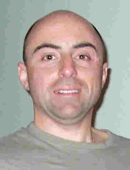
MICHAEL
RUBIN (Agilent Technologies, Fort Collins, CO)
|

|
Michael Rubin received the BSEE degree
from University of Kentucky, Lexington, KY, and MSEE from National
Technological University in 1994 and 2002 respectively. He worked in
IC manufacturing and design functions for Micron Technologies and Atmel
Corporation. In 1998, he joined Agilent Technologies IC Division,
where he was engaged in product engineering for advanced ASIC designs for
computer and communication markets. He was on a two-year assignment as
Product Engineering and EDA Manager with Agilent Technologies joint
venture, Chartered Silicon Partners, in Singapore. Currently, he is
RF IC Engineer in R&D with Agilent’s Wireless System Division in
Fort Collins, CO, working on the next generation of solid state RF
components for cellular markets. |
|
He published and presented number
of technical papers in the areas of product engineering and technical
management. His work interests
include advanced IC manufacturing, testing, and design technologies for
deep submicron memory, logic, RF, and embedded system products for
emerging technology markets. |
|