|
 |
|
|

Technical
Seminar Distinguished
Lecturer Series |
|
|
|
|
|
High-K Gate Dielectrics
|
|
|
DATE/TIME
Friday, August 5, 2005 (10:30am-12:00pm)
NOTE MORNING TIME!!! |
|
PLACE
Bldg. 1 Auditorium (Agilent Technologies,
Fort Collins, CO) |
|
DIRECTIONS
From I-25, take Harmony Road Exit (Exit
265) westbound, and enter Agilent/HP campus on right. Agilent/HP
campus is on the NE corner of Harmony Road and Ziegler Road.
Proceed to Bldg. 1 Lobby to sign-in and meet host for escort to Room
WLL2/3. |
|
Non-Agilent/HP/Intel
Attendees: Please arrive punctually at 10:15am as you will
need to be escorted to the seminar
room. We appreciate a courtesy RSVP to bob_barnes@agilent.com
to expedite sign-in and to help us with a headcount estimate for
food/drinks. |
|
|
ABSTRACT
Scaling gate oxide thickness of MOSFET
is known to improve short-channel effects, subthreshold
characteristics, drive current, and transconductance. However,
oxide scaling also leads to an increased gate leakage current and
standby power, degraded dielectric reliability and more severe
impurity penetration effects. High dielectric constant (high-K) thin
films might provide solution since physical thickness can be made
thicker while maintaining high capacitance. Hafnium-based
high-K dielectrics such as HfO2, HfON and HfSiON have
attracted a great deal of attention because of their potential for
successful integration into CMOS technology. However, channel
mobility degradation, charge trapping and reliability are major
concerns. In this presentation, we will discuss various
techniques (e.g. optimization of interfacial layer, incorporation of
N, Si, Al and La, high-temperature forming gas anneal and optimized
profiles) for improving channel mobility, EOT (equivalent oxide
thickness) scaling and reliability of high-K devices. Process
trade-off will be discussed in detail. For example, nitrogen
incorporation is known to reduce interfacial oxidation and thus
allows EOT scaling. However, it does result in higher
interface charge density and degraded mobility. Alternative
methods to achieve thinner EOT without N incorporation will also be
discussed. More recently, “higher-K” (i.e. K > 25) dielectrics
have been proposed in order to scale down EOT below 1.0nm. We
will review potential candidates and the challenges. We will
also present our recent experimental results of Hf-Ti-O dielectrics.
Finally, we will present the transient charge effects of high-K
dielectrics on CMOS inverter and ring oscillator operation. |
|
|
PROF. JACK
LEE (University of Texas, Austin, TX)
|
|
Jack C. Lee received the B.S.E.E. and M.S.E.E.
degrees from University of California, Los Angeles, in 1980 and 1981,
respectively; and the Ph.D.E.E. degree from University of California,
Berkeley, in 1988. He is a Professor of the Electrical and Computer
Engineering Department and holds the Cullen Trust For Higher Education
Endowed Professorship in Engineering at The University of Texas at
Austin. From 1981 to 1984, he was a Member of Technical Staff at the
TRW Microelectronics Center, CA, in the High-Speed Bipolar Device
Program. He worked on bipolar circuit design, fabrication and
testing. In 1988, he joined the faculty of The University of Texas
at Austin. His current research interests include thin dielectric
breakdown and reliability, high-K gate dielectrics and gate electrode,
high-K thin films for semiconductor memory applications, and semiconductor
device fabrication processes, characterization and modeling. He has
published over 250 journal publications and conference proceedings. Dr.
Lee has been awarded two Best Paper Awards, numerous Teaching/Research
Awards and several patents. Dr. Lee is a Fellow of IEEE. |
|
Website |
|
|
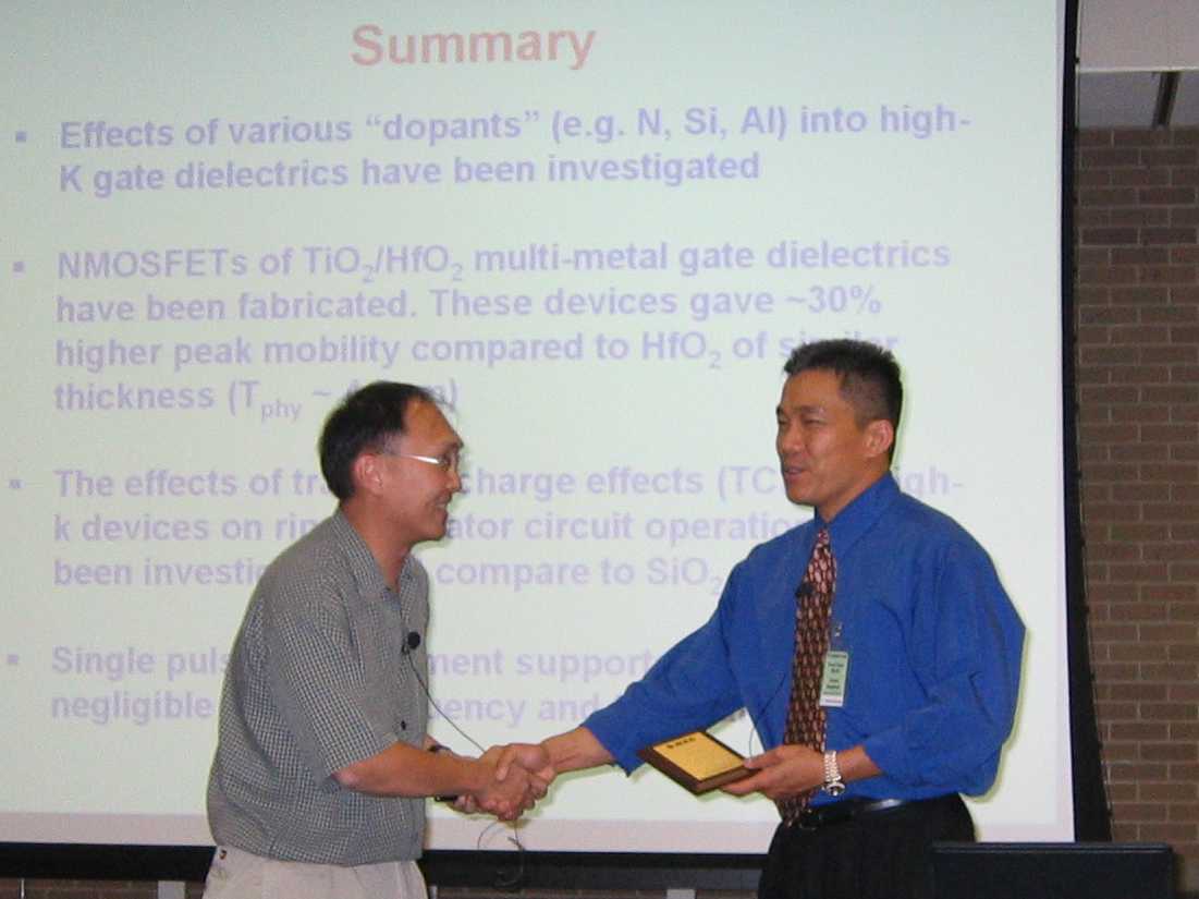
PHOTOS
Courtesy of Bob Barnes
|
|
 |
|
 |
|
 |
|