|
 |
|
|

Technical
Seminar |
|
|
|
|
|
Extreme Ultraviolet Light: Access to Nanometer
Geometries |
|
|
DATE/TIME
Thursday, October 11, 2007 (4:30pm to 6:00pm) |
|
PLACE
AMD Fort Collins Campus (Fort
Collins, CO)
|
|
DIRECTIONS
|
From I-25, take
Harmony Road Exit (Exit 265) westbound, AMD is a few miles west of the
exit, located on the NW corner of Harmony Road and Ziegler Road.
Proceed to 3rd floor for
escort to seminar auditorium. Non-AMD
employees: please arrive at 4:15pm for security sign-in and escort.
|
|
COST
Free. As always, food &
drinks will be provided. |
|
RSVP
Send e-mail to Tin Tin Wee at
tintin.wee@amd.com. |
|
|
ABSTRACT
|
|
Extreme ultraviolet (EUV) light is the name
given by the semiconductor industry to those wavelengths of light
between deep ultraviolet and X-rays. Not only extreme in
wavelength (13.4nm) but also in expense (at least double current costs)
, the technology is widely thought to be following immersion lithography
at 193nm and satisfy the International Technology Semiconductor Roadmap
for geometries below 22nm. Considerable development efforts in the
United States, Japan and Europe are taking place to solve some the steep
technical challenges while meeting the economic requirements.
Although the wavelength will again be shorter than the geometries being
defined, how much relaxation of the manipulations and computations for
generating mask sets and how well the device parameters will be
controlled is open to question. With geometries on integrated circuits
continuing to shrink and with a number of other materials being used in
the process increasing; the need for metrology for inspection and defect
identification continues to grow. In addition, on a wider scale,
the transition to nanometer geometries brings to the forefront
interesting material properties leading to films and devices with very
unique properties. The role of EUV in lithography, metrology and a
pathway to nanotechnology will be presented. Some highlights of
the research work at the EUV Engineering Research Center at CSU, CU, and
UC Berkeley will be shown. |
|
PRESENTATION SLIDES
pdf |
|
|
DR.
HUGH
GRINOLDS (Colorado State University, Fort Collins, CO)
|
 |
Hugh Grinolds is the industrial relations
officer for the NSF-funded EUV Engineering Research Center. He
also serves as an Adjunct Faculty member for Colorado State University,
teaching electronics and analog IC design. Dr. Grinolds has over
25 years experience in the semiconductor industry and has assumed
various scientist and management positions in research and development,
design, manufacturing and business management. In 1979, after
receiving a PhDEE from the University of Minnesota, he joined
Hewlett-Packard Laboratories in Palo Alto, CA, to work on CMOS device
design and GaAs ICs. He moved to
Corvallis, OR, and managed VLSI design for HP’s internal ASIC needs in
1988. He became the manufacturing manager in Fort Collins, CO, for
HP’s internal ASICs in 1993, responsible for the production of HP’s
PA-RISC processors and other ASIC’s for HP products and then |
|
assumed the role of world-wide manufacturing
manager in 1998. Moving with the business, he joined Agilent
Technologies in the spin off from HP in 1999. In 2002, he joined
Cymer Inc. and assumed responsibilities as an officer in the company and
managing the development of Extreme Ultraviolet sources. He came
back to Colorado in 2005 to explore business opportunities in Fort
Collins. He is
the author and co-author of a number of technical articles and several
patents. |
|
|
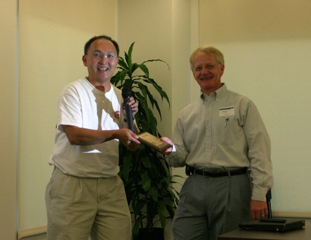
PHOTOS Courtesy of Tin Tin Wee |
|
 |
|
|
|