In this issue you will find two practical papers that
should be of interest to EMC engineers. The first, "EMC
Applications for Expert MININEC" describes a method
of moments computer program that has been used to solve
antenna problems for many years but that can also be used
to solve a number of very practical EMC problems. The
best news is that it can be downloaded for free from the
website indicated in the paper. I might add that even
if you don't intend to use the program, the section on
its history is worth reading. Finally, since your Technical
Editor is one of the authors, I asked Colin Brench of
Hewlett Packard to serve as the acting Technical Editor
for this paper and want to thank him for his excellent
service. The second paper is entitled, "Numerical
EMC Simulation for Automotive Applications" and is
by several authors from Austria and Germany. As the automotive
industry increases its use of electronic control systems,
EMC issues naturally emerge. I think that you will find
this to be an interesting introduction to some of the
EMC problems that are faced when designing modern automobiles.
This paper was first presented at the 2003 International
Zurich Symposium on Electromagnetic Compatibility and
has been reprinted here by permission.
The purpose of this section is to disseminate practical
information to the EMC community. In some cases the material
is entirely original. In others, the material is not new
but has been made either more understandable or accessible
to the community. In others, the material has been previously
presented at a conference but has been deemed especially
worthy of wider dissemination. Readers wishing to share
such information with colleagues in the EMC community
are encouraged to submit papers or application notes for
this section of the Newsletter. Click
here for my e-mail. While all material will be reviewed
prior to acceptance, the criteria are different from those
of Transactions papers. Specifically, while it is not
necessary that the paper be archival, it is necessary
that the paper be useful and of interest to readers of
the Newsletter.
Comments from readers concerning these papers are welcome,
either as a letter (or e-mail) to the Associate Editor
or directly to the authors.
|
EMC Applications for Expert MININEC
J. W. Rockway, J. C. Logan
Space and Naval Warfare Systems Center - San Diego
R. G. Olsen
Washington State University
Abstract
A brief description is given of the Expert MININEC
wire antenna modeling code. Two examples of the EMC applications
of this code are described.
Expert MININEC Description
The sample problems described in this paper were analyzed using
Expert MININEC Classic. Expert MININEC
Classic is available for free and can be downloaded from the
following web site:
https://www.emsci.com/
Expert MININEC Classic is a limited
version of the more general codes available on the same web site.
Nevertheless, it is a powerful code useful for many practical
problems such as the ones described in this paper. For example,
it allows the use of up to 500 wires and 1250 unknowns; far more
than needed to solve the problems described here. Other limitations
of Expert MININEC Classic will be explicitly indicated
within the text of this paper.
Expert MININEC is an advanced engineering tool for
the design and analysis of wire antennas. The process of solution
begins with several assumptions that are valid for thin wires.
These assumptions include that the wire radius is very small with
respect to the wavelength and is very small with respect to wire
length. Because it is necessary to subdivide wires into short
segments, the radius should also be small with respect to the
segment length, so that currents can be assumed to be axially
directed (i.e., there is no azimuthal component of the current).
Expert MININEC solves for currents on thin wires
using a Galerkin procedure applied to an electric field integral
equation. The electric field is formulated in terms of its scalar
and vector sources. These sources are the vector magnetic potential
and the scalar electric potential. The two potentials can be calculated
from potential integrals, which are solutions of the Helmholtz
vector and scalar wave equations. In the potential integrals,
the integrands are the wire current and wire charge distributions.
The current and charge are linked via the equation of continuity.
Expert MININEC makes use of the boundary condition
on tangential electric fields at the surface of a perfect conductor,
namely that the electric field must be zero. Since the wires are
assumed to be thin, this forces the total axial electric field
on the wire to zero. The three sources of the tangential electric
field on the wire are:
-
Currents and charges on the wires and on
nearby wires.
-
Incoming waves from distance or nearby radiators.
-
Local sources of electric field on the wire.
The local sources are usually in the form of
voltage sources, current sources, or transmission lines that connect
to the wires. By summing the tangential electric field components
at each segment on the wire and enforcing the zero total value,
an integral representation for the currents and charges is obtained.
The integral equation relating the tangential electric field at
the surface of a perfect conductor and the vector and scalar potentials
is
 (1) (1)
where
 (2) (2)
and
 (3) (3)
are the vector and scalar potentials respectively.
The integration is along the length S of the wire and
 (4) (4)
r is the distance from the source point of the current to the
observation point of the field. The integration is over the angular
variation around the wire. From the continuity equation, the linear
charge density is
 (5) (5)
Application of the method of moments to this formulation results
in an unusually compact and efficient computer algorithm. A matrix
equation is generated that is used to solve for the currents on
the thin wires.
The user interface to Expert MININEC is through
Microsoft Windows. Input data screens provide format sensitive
entry boxes in individual windows with tabular data displays.
Expert MININEC modeling geometry constructs include:
(An * indicates that this feature is not available in Expert
MININEC Classic.)
-
Cartesian, cylindrical and geographic coordinate
systems
-
Meters, centimeters, feet or inches selection
-
Straight, curved*, helix*, spiral*, and
catenary* wires
-
Wire meshes*
-
Automated canonical structure meshing*
-
Node coordinate stepping
-
Symmetry options*
-
Rotational and linear transformations *
-
Numerical Green's Function*
-
Automated convergence testing*
Electrical description options include:
-
Free space, perfect ground, and imperfect
ground environments
-
Frequency stepping
-
Loaded wires
-
Lumped loads
-
Passive circuits*
-
Transmission lines*
-
Voltage and current sources
-
Plane wave source excitation*
Solution description options include:
In addition, the Expert MININEC
includes a user-oriented capability to analyze finite arrays within
the limits of Expert MININEC capabilities.*
Output products are displayed in both tabular and graphics forms.
The integrated graphics of Expert MININEC include:
-
3-D geometry displays with rotation, zoom
and mouse support.
-
3-D currents, charges and pattern displays.
-
Linear, semilog and log-log plots of currents,
coupling, near fields, impedance and admittance.
-
Smith Chart plots of impedance and admittance.
-
Linear and polar pattern plots.
Input and output data screens are fully interfaced
to Windows printer drivers as well as other window applications,
such as word processors and spread sheets. On-line, context sensitive
help is also provided.
The computational intensive algorithms are implemented in FORTRAN
for greater speed and make maximum use of available memory to
set array sizes. The formulation has been changed from earlier
versions of the MININEC to use triangular basis functions. This
results in greater accuracy. The short segment limit is a function
of machine accuracy. Square loops and Yagi antennas may be solved
with confidence. In addition, a Fresnel reflection coefficient
approximation improves the calculation of currents in the vicinity
of real ground for wire segments more than one-tenth of a wavelength
from the ground. As a summary Expert MININEC solves
for
-
Currents and charges on wires (peak or RMS)
-
Impedance, admittance, S11 and S12
-
Effective height and current moments
-
Power losses and load voltages *
-
Multi-port (antenna-to-antenna) coupling
-
Near electric and magnetic fields
-
Radiation patterns (dBi or electric fields,
power or directive gain)
-
Medium wave array design *
-
Auxiliary calculations of ground wave, stub
matching, and tower footing impedance*
Expert MININEC Development
History
The original MININEC was written by John Rockway with a little
prodding and support from Jim Logan. Over the years, the Rockway
- Logan team has been responsible for the development of this
code into one of the best known and most useful Method of Moments
antenna modeling codes available. A number of other individuals
have also contributed small, but not necessarily insignificant,
pieces to the MININEC capability, but it has been the dual efforts
of the Rockway - Logan team that has made MININEC into a powerful
antenna design and analysis tool.
Because of the similarity in names, it is often stated that MININEC
is but a personal computer (PC) version of its big brother, NEC
[2]. However, this could not be farther from the truth. There
are significant differences between these two codes. Both codes
use the Method of Moments to solve for currents on electrically
thin wires. However, each code starts with a different version
of the integral formulation for the currents and fields for wires.
Then, each follows significantly different algorithms for implementation
of the Method of Moments.
In 1980, when the first version of MININEC was written, PCs had
not been on the market for very long. They were relatively expensive
and very limited in capability. PCs were generally regarded as
mere novelties or toys. PCs were typically limited to 16K memory
with a 8 bit word length. There was no FORTRAN. MININEC had to
be written in BASIC. NEC was (and still is) a very powerful computer
code, with tens of thousands of FORTRAN statements, originally
written for use on large main frame computers. In those days PCs
could not support such a large program size. The formulation had
to be changed to allow a simpler implementation of the Method
of Moments in order to produce a more compact code. It would not
be possible to include many of the powerful modeling options provided
by NEC. Following the advice of Professor Don Wilton at the University
of Mississippi (now with the University of Houston), the first
version of MININEC was written in 500 lines BASIC and required
32k of memory. Nonetheless, this version proved surprisingly accurate
for dipoles and monopoles.
The first public release of MININEC occurred in 1982 [3]. The
code was 550 lines of BASIC and would run on an APPLE II computer
with 64 kilobytes of memory. It could compute the current distribution,
impedance, and far field pattern of an arbitrarily oriented set
of wires in free space or over a perfectly conducting ground plane.
Lumped impedance loads were allowed at segment junctions except
for segments intersecting with the ground plane. Also, wires intersecting
the ground plane were restricted to right angles. In interpreter
BASIC (there were no BASIC compilers then) the problem size was
limited to 10 wires and 50 currents (or 70 segments with junctions).
MININEC was an instant success. Almost immediately, a small user
group developed and began to grow. In 1984, partly to meet the
demand for MININEC as well as share other computer algorithms,
the authors teamed up with two colleagues, Peter Li and Dan Tam.
They published a book that contained an improved version of MININEC
along with some other useful algorithms [5]. MININEC2, as it became
known, was not significantly different from its predecessor, but
the limitation for wires intersecting the ground plane was removed.
Wires could intersect the ground at any angle.
The power of PCs began to grow. Computers were getting faster,
had more memory, and utilized math coprocessors. BASIC compilers
also became available. These factors opened up new vistas for
MININEC. In 1986, the authors released MININEC3 [6]. This code
featured a new user interface which automatically determined wire
connections from the user inputs for wire end coordinates. It
could also read and interpret a limited NEC input data set. However,
there was no way to save and edit geometry data. MININEC3 included
near fields, a Fresnel reflection coefficient correction to the
patterns for real ground, and an expanded lumped parameter loading
option. MININEC had grown to just over 1600 lines of BASIC. With
a math coprocessor and a BASIC compiler, MININEC3 could solve
antenna problems up to 50 wires and 50 current unknowns.
The next MININEC effort by the authors produced the MININEC SYSTEM
in 1988 [8]. This was a valiant effort by the authors to provide
improved problem definition, save features, and on-line graphics.
The release of the MININEC SYSTEM happened to coincide with the
introduction of Microsoft Windows that took the PC world by storm.
The authors were too close to publication to backtrack and implement
a Windows system. However, there were many worthwhile innovations
represented in this code. This was the first version of MININEC
that required a compiler, a BASIC compiler. Previous versions
could be run in interpreter BASIC. The solution time and storage
requirements for rotationally symmetric antennas were greatly
reduced. The transpose elimination algorithm was available as
a user select option to allow computation of larger problems,
up to 50 wires and 90 current samples or 190 segments were permitted
without recompiling.
Many others have also attempted to improve on MININEC. Most notable
are the innovative user interfaces and graphics displays offered
by Roy Lewallen [4] in 1991 and Brian Beezley [1] in 1992.
In 1995, the authors published the first of a series of MININEC
for Windows codes. These codes represented the development of
a new version of MININEC. An improved solution of the potential-integral
formulation for the currents resulted in a more accurate formulation
in the solution for the currents on wires. In addition, FORTRAN
was used for the computationally intensive portions of MININEC.
This led to an increase in speed over previous versions of MININEC.
The first code was MININEC Professional for Windows [9]. Because
it is a Windows application, text and graphical outputs are easily
transferred to other Windows applications such as spreadsheets
and word processors. Mouse support and printer drivers are also
supplied by the Windows environment. The input is a node based
geometry. That is, nodes define points in space (in Cartesian,
cylindrical or geographic coordinates) and wires are defined between
nodes. Entries are made in tables through individualized window
screens. On line, context sensitive help is provided along with
diagnostic preprocessing diagnostics. MININEC Professional
is dimensioned for 1000 wires and 2000 unknowns.
In 1996, the authors published MININEC Broadcast Professional
for Windows [10] which is similar to its predecessor, but more
powerful. Additional features include an improved voltage source
model, a plane wave source model, automated convergence testing,
design analysis post processing, array synthesis, and ground wave
calculations. MININEC Broadcast Professional is dimensioned
for 2000 wires and 4000 unknowns.
Also in 1996, the authors published MININEC for Windows
[11], a simplified version of MININEC Professional which
is more suitable to first time users and their pocketbooks. This
code is dimensioned for 400 wires and 800 unknowns.
In 1999, the authors published another improved set of codes,
the Expert MININEC Series [12][13][14]. The new
series features "Expert" assistance in selecting appropriate
input dialog boxes while constructing a model. Context sensitive
help is still an important feature. Accuracy and speed have also
been improved.
Example 1 - Antenna Coupling
Antenna modeling codes, such as Expert MININEC can
be used to accurately and efficiently calculate the coupling between
antennas. Antenna coupling is a significant parameter in many
electromagnetic compatibility (EMC) analyses. The specific approach
is based on an N-port description and the application of the Linville
method [15].
N-port Description
When two or more antenna systems are in proximity to each other,
power from a transmitting system can be coupled into the other
systems through an electromagnetic interaction. The problem of
coupling among the antenna systems can be described using network
"Y" parameters [16]. Any two ports of an antenna can
be treated as a two-port network of the electromagnetic interactions.
In the Figure 1 the terminals with voltage Vi are the
feedpoint of antenna port i, and the terminals j are the feed
point of the second antenna port. By convention, the currents
Ii and Ij are assumed to be positive into
the electromagnetic interaction network.
In general, of the four variables shown (Vi, Ii,
Vj, Ij), only two are independent. Thus,
the following functions may be written:
 (6) (6)
 (7) (7)
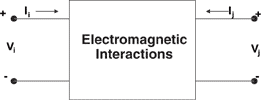 |
| Figure 1. Two-port Electromagnetic
Interaction Network Definition. |
Since the electromagnetic interactions are passive
and linear, the functions can assumed to be linear and thus:
 (8) (8)
 (9) (9)
These admittance parameters are defined by:
 (10)
(10)
 (11) (11)
 (12) (12)
 (13) (13)
Vi and Vj equals zero implies that the terminals
associated with these voltages are short-circuited. An arrangement
whereby these admittances may be computed is shown in Figures
2 and 3.
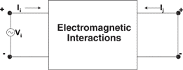 |
| Figure 2. Arrangement for Determining
Yii and Yji. |
 |
|
Figure 3.
Arrangement for Determining Yjj and Yij.
|
The feed point of one electromagnetic port is
excited, and the feed point of the second electromagnetic port
is short-circuited. The calculated currents are used with equations
(10) through (13) to determine Yii, Yji,
Yij, and Yjj. It has been found that the
admittance port parameters can be computed more effectively with
the Method of Moments solution of the electromagnetic interactions.
Once the admittance port parameters have been found, the maximum
coupling between ports can be determined.
Linville Method
Again consider Figure 2 and assume a load ,Yload, on
port j instead of a short circuit. The output power is
 (14) (14)
where Vj is the output voltage (port j), and
Re [Yload] is the real part of the load admittance
. The input power is
 (15) (15)
where Vi is the input voltage (port i), Re [Yin]
is the real part of the input admittance of port i.
The power gain is then the ratio of (14) and (15)
 (16) (16)
This ratio is dependent on the input admittance. Yin can be calculated
from Equation (8) and (9) by solving
 (17) (17)
with
 (18) (18)
then
 (19) (19)
It is noted that Yin depends on the load Yload.
The two-port admittance parameters in Equations (8) and (9) can
be used also to find the output to input voltage ratio, , as follows
 (20) (20)
Substituting ((20)) into ((16)), the gain becomes
 (21) (21)
The load admittance, Yload, can be
found that maximizes the gain. This gain is the maximum possible
power transfer ratio, provided that the generator is matched to
the resulting Yin as given in (19).
It is difficult to maximize the gain directly by taking the derivative
of Equation (21) with respect to complex load admittance, Yload,
and setting the derivative to zero. A more appropriate method
is the Linville analysis approach used in the design of RF amplifiers
[16]. The Linville method is a graphical based method. Using the
Linville approach, the maximum coupling becomes
 (22) (22)
where
 (23) (23)
The matched load admittance on port j for the
maximum coupling is
 (24) (24)
where
 (25) (25)
and * indicates complex conjugate of the product
of Yij and Yji.
The maximum coupling between ports can be used to identify the
greatest coupling paths. The maximum coupling calculation can
be used to rank order the interactions. Possibly, this rank ordering
can be used to eliminate the more weakly coupled paths as not
being significant to the EMC analysis. This rank order provides
insight into the design.
Example Calculation
As an example calculation, consider two monopoles. Each monopole
has a length of .25 meters and a radius of .001 meters. The antennas
are .1 meters apart. Six segments are used for each monopole in
the Method of Moments calculation. The problem is to determine
the maximum coupling between the two monopoles from 260 MHz to
350 MHz. As an example, at 260 MHz, the current computation for
a one volt source on the first antenna is given in the following:
Current peak real
imaginary
no. X
Y
Z
(amps)
(amps)
GND -.05 0
0 5.57E-03
.0163887
2
-.05 0
.0416667
5.41E-03 .0149296
3 -.05
0
.0833333 4.93E-03
.0129975
4
-.05 0
.125
4.15E-03
.0104939
5
-.05 0
.166667
3.08E-03 7.49E-03
6
-.05
0
.208333 1.74E-03 4.06E-03
END -.05
0
.25 0
0
GND
.05
0
0 4.78E-03
-6.53E-03
8 .05
0
.0416667 4.64E-03 -6.31E-03
9
.05 0
.0833333 4.23E-03 -5.68E-03
10
.05
0
.125 3.57E-03
-4.67E-03
11
.05
0 .166667
2.65E-03 -3.36E-03
12 .05
0 .208333
1.5E-03 -1.83E-03
END
.05
0
.25 0
0
The current computation for a one volt source
on the second antennas is given in the following:
CURRENT peak real
imaginary
no. X
Y
Z
(amps) (amps)
GND -.05 0
0 4.78E-03
-6.53E-03
2
-.05 0
.0416667 4.64E-03 -6.31E-03
3 -.05
0
.0833333
4.23E-03 -5.68E-03
4 -.05
0
.125
3.57E-03
-4.67E-03
5
-.05
0
.166667 2.65E-03 -3.36E-03
6
-.05 0
.208333 1.5E-03
-1.83E-03
END -.05
0
.25 0
0
GND
.05
0
0 5.57E-03
.0163887
8
.05
0
.0416667 5.41E-03
.0149297
9 .05
0
.0833333 4.93E-03
.0129976
10 .05
0
.125 4.15
E-03 .0104939
11
.05 0
.166667 3.08E-03 7.49E-03
12
.05 0
.208333 1.74E-03 4.06E-03
END .05
0
.25
0
0
The appropriate admittance parameters are calculated
using Equations (10) to (13). Since there is obvious symmetry
for this problem, the admittance parameters are
Y11 = Y22 = .00557 + j .0163887
Y12 = Y21 = .00478 -j .00653
Equation (22) is then used to calculate the maximum coupling.
The load for this maximum coupling is given by Equation (24).
Finally, the input impedance for this load is given by Equation
(19). The results for an Expert MININEC calculation
are given in the following table:
frequency input impedance
load impedance
coupling
(MHz) (ohms)
(ohms) (ohms)
(ohms) (dB)
260. 8.78226
-43.6793 8.78229 43.6792
-3.01957
270. 10.1627 -29.1595
10.1627 29.1594 -3.14462
280. 11.7534 -14.6924
11.7534 14.6925 -3.26634
290. 13.5772
-.184137 13.5772 .183732
-3.38805
300. 15.6652 14.4604
15.6652 -14.4604 -3.51159
310. 18.0553 29.336
18.0554 -29.3361 -3.63828
320. 20.7965 44.5426
20.7966 -44.5423 -3.7687
330. 23.9493 60.1861
23.9493 -60.186
-3.90311
340. 27.5894 76.38
27 .5894 -76.38
-4.04161
350. 31.8117 93.2499
31.8117 -93.2497 -4.18412
Example 2 - Common Mode Radiation
Common mode radiation is a concern for EMC engineers since it
is often a much more serious problem than differential mode radiation.
If the structure of interest is a multiconductor transmission
line with a conductive return path (e.g., a two wire transmission
line over a ground plane), it is possible to calculate the common
and differential mode currents using conventional multiconductor
transmission line theory [7]. This technique is well known to
EMC engineers. Less well known, however, is how to determine these
currents when the current return path is not conductive. For this
case full wave electromagnetic theory must be used. The purpose
of this example is to illustrate how an antenna analysis program
such as Expert MININEC can be used to determine
common mode current amplitudes.
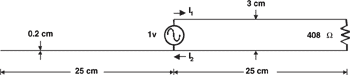
Consider first the simple problem shown in the following figure.
Here, a balanced transmission line is driven by a 1 volt sinusoidal
source and terminated by a 408 _ resistor that matches the characteristic
impedance of the transmission line. The transmission line is 25
cm in length and constructed with .2 cm diameter wires spaced
3 cm apart. The currents I1 and I2 represent the currents into
and out of the top and bottom wires respectively.
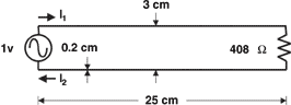 |
|
Figure 4.
Open Wire Transmission Line Terminated in its Characteristic
Impedance.
|
Note here that the definitions of common mode, Ic, and differential
mode, Id, currents are respectively
 (26) (26)
 (27) (27)
Because the geometry of the problem is symmetric,
I1 = I2 for all frequencies, the current
is entirely differential. This result is consistent with two wire
transmission line theory. This has also been demonstrated directly
using Expert MININEC over the frequency range of
interest, 10 to 300 MHz. For the Expert MININEC
calculation, each horizontal wire was divided into 40 segments
and the vertical wires divided into 3 segments.
If, however, another wire that might represent a ground lead that
extends past the source is added, the symmetry of the problem
is destroyed. This geometry is depicted in Figure 5. In this case,
two wire transmission line theory is not appropriate and an analysis
tool such as Expert MININEC must be used.
 |
|
Figure 5.
Open wire transmission line with an additional wire to the
left side.
|
The results of this calculation are shown in Figure 6. It is clear
that at lower frequencies, the differential mode dominates since
little current flows through an open circuited, electrically short
wire. At these lower frequencies, conventional transmission line
theory that assumes differential mode currents can be used despite
the lack of symmetry. However, as the length of the structure
approaches a half wavelength, the common mode current becomes
significant. In fact, it can actually dominate the differential
mode current. In this case, the structure behaves more like an
antenna than a transmission line.
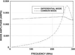 |
| Figure 6. Common and differential
mode currents on the structure of Figure 5. |
References
1. Beezley, B., The MN4 Manual, Brian Breezley, Vista, CA, 1992.
2. Burke, G. J. and A. J. Poggio, "Numerical Electromagnetics
Code (NEC) - Method of Moments," Naval Ocean Systems Center
Technical Document 116, January 1981.
3. Julian, A. J., J. C. Logan, J. W. Rockway, "MININEC: A
Mini-Numerical Electromagnetics Code," NOSC Technical Document
516, September 1982.
4. Lewallen, R., "MININEC: The Other Edge of the Sword,"
QST Magazine, February 1991.
5. Li, S. T., J. C. Logan, J. W. Rockway, D. W. Tam, Microcomputer
Tools for Communications Engineering, Artech House, Inc., Dedham,
MA 1984.
6. Logan, J. C. and J. W. Rockway, "The New MININEC (Version
3): A Mini-Numerical Electromagnetic Code," NOSC Technical
Document 938, September 1986.
7. Paul, C. R., Introduction to Electromagnetic Compatibility,
Wiley, New York, 1992
8. Rockway, J. W., J. C. Logan, D. W. Tam, and S. T. Li, The MININEC
System: Microcomputer Analysis of Wire Antennas, Artech House,
Inc. Dedham, MA 1988.
9. Rockway, J. W. and J. C. Logan, MININEC Professional for Windows,
EM Scientific, Inc., Carson City, Nevada, 1995.
10. Rockway, J. W. and J. C. Logan, MININEC Broadcast Professional
for Windows, EM Scientific, Carson City, Nevada, 1996.
11. Rockway, J. W. and J. C. Logan, MININEC for Windows, EM Scientific,
Carson City, Nevada, 1996.
12. Rockway, J. W. and J.C. Logan, Expert MININEC Professional
for Windows, EM Scientific, Inc., Carson City, NV, 1999.
13. Rockway, J. W. and J.C. Logan, Expert MININEC Broadcast Pro
for Windows, EM Scientific, Inc., Carson City, NV, 1999.
14. Rockway, J. W. and J.C. Logan, Expert MININEC for Windows,
EM Scientific, Inc., Carson City, NV, 1999.
15. Rubin, D., "The Linville Method of High Frequency Transistor
Amplifier Design," Naval Weapons Center, Research Department,
NWCCL TP 845, Corona Laboratories, Corona, California, March 1969.
16. Van Valkenburg, M. E., Modern Network Synthesis, John Wiley
and Sons, New York 1960.
 John
Rockway received the B.S. and M.S. degrees in electrical engineering
and Ph.D. in engineering science from Washington State University
in 1966, 1968 and 1971, respectively. He is currently the head
of the technical staff of the Electromagnetics and Advanced Technology
Division of the Space and Naval Warfare Systems Center - San Diego
(SSC-SD). He has spent his entire engineering career with SSC-SD
and its predecessors. The primary emphasis of this career has
been on the development and evaluation of shipboard antennas,
development and application of advanced computational electromagnetic
and RF system design tools, and the development of advanced communication
systems for the Navy. Government and professional recognitions
include IEEE Fellow, the Lauritsen-Bennett Award (SSC-SD highest
honorary award for Excellence in Engineering), the Department
of the Navy Award for Meritorious Civilian Service, the National
Society of Professional Engineers Federal Engineer of the Year
Award and the Applied Computational Electromagnetics Society Mainstay
Award. John
Rockway received the B.S. and M.S. degrees in electrical engineering
and Ph.D. in engineering science from Washington State University
in 1966, 1968 and 1971, respectively. He is currently the head
of the technical staff of the Electromagnetics and Advanced Technology
Division of the Space and Naval Warfare Systems Center - San Diego
(SSC-SD). He has spent his entire engineering career with SSC-SD
and its predecessors. The primary emphasis of this career has
been on the development and evaluation of shipboard antennas,
development and application of advanced computational electromagnetic
and RF system design tools, and the development of advanced communication
systems for the Navy. Government and professional recognitions
include IEEE Fellow, the Lauritsen-Bennett Award (SSC-SD highest
honorary award for Excellence in Engineering), the Department
of the Navy Award for Meritorious Civilian Service, the National
Society of Professional Engineers Federal Engineer of the Year
Award and the Applied Computational Electromagnetics Society Mainstay
Award.
 Mr.
James C. Logan earned his BSEE degree in 1967 and his MSEE
degree in 1973, both from Syracuse University. He was a co-founder
of the Applied Computational Electromagnetics Society (ACES) in
1984. During the first 10 years of ACES, Mr. Logan served as the
first Vice President, the second President and the second Treasurer
as well as numerous committees. He is also a Senior Member of
the International Institute of Electrical and Electronics Engineers
(IEEE) Antennas and Propagation Society and the IEEE Electromagnetic
Compatibility Society. Mr. Logan is the author or co-author of
many (more than 60) papers and presentations appearing in professional
publications as well as numerous Government documents. Mr. Logan
is also co-author of five commercial books; one on the design
and analysis of RF communications systems and four on the design
and analysis of antennas. Mr. Logan co-founded EM Scientific,
Inc. in 1995. EM Scientific, Inc. is a publisher of scientific
and engineering software and reference books. Mr. Logan retired
from the Space and Naval Warfare Systems Center - San Diego (SSC-SD)
in 1999. He is now a retired annuitant at SSC-SD. Mr.
James C. Logan earned his BSEE degree in 1967 and his MSEE
degree in 1973, both from Syracuse University. He was a co-founder
of the Applied Computational Electromagnetics Society (ACES) in
1984. During the first 10 years of ACES, Mr. Logan served as the
first Vice President, the second President and the second Treasurer
as well as numerous committees. He is also a Senior Member of
the International Institute of Electrical and Electronics Engineers
(IEEE) Antennas and Propagation Society and the IEEE Electromagnetic
Compatibility Society. Mr. Logan is the author or co-author of
many (more than 60) papers and presentations appearing in professional
publications as well as numerous Government documents. Mr. Logan
is also co-author of five commercial books; one on the design
and analysis of RF communications systems and four on the design
and analysis of antennas. Mr. Logan co-founded EM Scientific,
Inc. in 1995. EM Scientific, Inc. is a publisher of scientific
and engineering software and reference books. Mr. Logan retired
from the Space and Naval Warfare Systems Center - San Diego (SSC-SD)
in 1999. He is now a retired annuitant at SSC-SD.
Professional awards and recognitions include:
-
Applied Computational Electromagnetic Society,
1990 Mainstay Award.
-
Naval Surface warfare Center, Caderock Division,
Group Award Citation for leadership and determination in defining
and developing the Advanced Enclosed Mast/Sensor System (AEM/S),
June 10, 1994.
-
Applied Computational Electromagnetic Society,
1994 Founders Award.
-
Naval Command, Control and Ocean Surveillance
Center Exemplary Achievement Award, June 16, 1997.
-
Naval Surface Warfare Center, Caderock Division,
Incentive Award for Special Act or Service, December 10, 1997.
-
Department of the Navy, Navy Meritorious
Civilian Service Award, June 26, 1998.
-
The Chief of Naval Research Dr. Arthur E.
Bisson Prize for Naval Technology Achievement, May 16, 2000.
 Robert
G. Olsen (S'66 - F'92) received the BS degree in electrical
engineering from Rutgers University in 1968 and the MS and Ph.D.
degrees in electrical engineering from the University of Colorado,
Boulder in 1970 and 1974 respectively. Robert
G. Olsen (S'66 - F'92) received the BS degree in electrical
engineering from Rutgers University in 1968 and the MS and Ph.D.
degrees in electrical engineering from the University of Colorado,
Boulder in 1970 and 1974 respectively.
Prof. Olsen has been a member of the electrical engineering faculty
at Washington State University since 1973. During that time he
has been a visiting scientist at GTE Laboratories in Waltham,
MA at ABB Corporate Research in Västerås, Sweden and
at EPRI in Palo Alto, CA and a Visiting Professor at the Technical
University of Denmark.
His research interests include electromagnetic interference from
power lines, the electromagnetic environment of power lines, electromagnetic
wave propagation, electromagnetic compatibility and electromagnetic
scattering. His recent work has been supported by the Bonneville
Power Administration, the Boeing Defense and Space Group, the
Electric Power Research Institute, the National Science Foundation
and the U.S. Navy.
He is a Fellow of the IEEE and presently serves as chair of the
IEEE Power Engineering Society Corona Effects Fields Working Group,
as Technical Editor of the IEEE Electromagnetic Compatibility
Society Newsletter and as USNC representative to CIGRE Study Committee
36 (Electromagnetic Compatibility). He is past chair of the IEEE
Power Engineering Society AC Fields Working Group.
Errata
Art Glazar, author of the article, "A
Software Implementation of TL Field-to Cable Coupling
Equations," that appeared in the Fall 2000 issue
of the Newsletter has informed us that the computer program
(coax.exe) offered for free in that article has an error
that affects problems where shields or signals are terminated
by a complex impedance. He has corrected the error and
will send an updated version of the program to anyone
who requests it. If you would like to have this, please
e-mail him at aglazar@ieee.org
|
NUMERICAL EMC SIMULATION
FOR AUTOMOTIVE APPLICATIONS
R. Neumayer1, A. Stelzer1, F.
Haslinger2, G. Steinmair2, M. Tröscher3,
J. Held4, B. Unger4, R. Weigel5
1University Linz, Austria; 2BMW AG, Germany;
3SimLab Software GmbH, Germany;
4SIEMENS AG, Germany; 5University Erlangen-Nuremberg,
Germany
(Principal contact: roland.neumayer@ieee.org)
Abstract: New electronic systems accompany most of the
technical innovations in automotive industry. In consequence of
the growing number of electrical equipment the electromagnetic
noise level is rising in automobiles. The increased electromagnetic
emissions however raise the risk to miss EMC standards and perturb
the functional integrity of new and existing electronic systems.
Hence, mastering potential EMC problems in new automobiles becomes
increasingly important to the car industry.
Numerical simulation is an important key for the detection and
rejection of potential EMC problems early in the design process.
This paper presents a continuous concurrent EMC simulation process
based on the exchange of EMC models between car manufacturer,
electronic supplier and IC developer. The described process fundamentally
influences the introduction of new technologies in a vehicle by
cutting the risk of EMC failure and avoiding costly and time-consuming
redesigns.
1. Introduction
In recent years there has been a significant increase in the amount
of electronics that have been introduced into the car and this
trend is expected to continue as car companies introduce further
advances in safety, reliability and comfort. The accompanying
increase of electronic noise emission and interference is a well-known
problem in the automotive industry [1]. In modern cars, the expenses
for the control of the electromagnetic emission per car can add
up to 50 Euro for preventive measures such as filters and wire
shielding. The costs of the chip manufacturer and the electronic
supplier for electromagnetic compatibility (EMC) corrections are
not included in the above amount.
In addition, future technical developments, such as:
-
an increasing number of pulse-width-modulated
(PWM) signal applications for electrical consumers (especially
in 42Volt systems),
-
wider penetration of the harness through
the car,
-
higher data traffic (new bus systems tend
to data transmission rates up to 10Mbits/s using standard twisted
pair cables), will aggravate EMC problems in automotive applications
and increase the need for early detection and rejection of potential
EMC failures.
Currently, system-level automotive EMC is controlled
in two steps. In the first step, the electrical components inside
a car are tested according the corresponding international standards
(e.g. ISO7637 Part 2 and 3) and the standards of the car manufacturer.
In the second and final step, system-level EMC tests (e.g. EN95/54/EG)
on the car are performed. The mentioned standards describe measurements
to qualify the electromagnetic noise emission and immunity. These
measurements are performed on existing hardware at the end of
the development process. The standards reflect the experience
of the EMC engineers with existing electronics.
The latter two points, however, indicate the major drawbacks in
the current EMC design flow. First, the existing standards are
frequently insufficient for new electronic systems integrated
in the car, e.g. a neon lamp can fulfill the standard for EM emission,
but built in the rear window as a third brake light, it can inhibit
any radio reception with the rear window antenna. Second, since
the EMC problems are treated in a late stage of design or during
prototype testing, correction measures are limited and usually
cost-intensive. In the worst case, repeated redesign cycles for
the automobile might stack up to several months and the introduction
of new products to the market can be delayed dramatically.
Consequently, an accurate analysis of potential EMC problems in
new automobiles, such as:
-
coupling between wires inside a harness
(crosstalk),
-
radiation from the harness towards the environment
and antenna (emission),
-
immunity of equipment against external electromagnetic
interference (immunity), in earlier stages of the development
process is increasingly important to the car industry.
Numerical EMC simulation is an important key
to reach this aim [2]. This paper describes a continuous, concurrent
EMC simulation process developed under the COSIME project, granted
by the European Commission. In Section 2, the general modeling
and simulation strategy based on the exchange of EMC models between
car manufacturer, electronic supplier, and chip developer is explained.
Section 3 discusses different modeling approaches at sub-system
level, while Section 4 presents how to perform the final system-level
EMC simulation. In Section 5 the validation of the proposed process
is discussed. Conclusions are drawn in Section 6.
2. Continuous Concurrent EMC Simulation
Previous considerations place the demand for a design process
that comprises EMC analysis from the early development phase and
guarantees that the final product performs as requested, without
the need of adjustments during the prototype and production phase.
Employing numerical EMC simulation throughout all design stages
enables the targeted early identification of potential system
malfunctions and most appropriate correction measures can be placed
in time.
EMC simulation is well advanced in the development process of
automotive electronics. Like the EMC validation by means of measurements,
the EMC simulation is divided into the fields of electromagnetic
emission (EMI) and electromagnetic susceptibility (EMS). Besides,
it is distinguished between component simulations and system simulations
at car level. The component simulations are less complex in principle,
since no geometrical data of the car is needed and the test concerns
only single components. The efficiency of this simulation process
has already been proved [3, 4].
The complete car simulation, however, is still considered a challenge.
One major difficulty encountered in automotive EMC simulation
is to deal with very different relevant geometric scales, related
to the three main parts of the problem: the car body (large 3D
structures), the harness (2D incorporating ground plane effects),
and the equipment (essentially 0D). This scattering of geometric
scales corresponds to different physical behaviors, which consequently
call for different modeling approaches and different simulation
environments [5] such as:
-
full-wave 3D resolution at the car body
level (incl. antenna),
-
transmission line propagation at harness
and bundles level, and
-
circuit formulation for equipment of negligible
size with respect to the wavelength of interest.
Applying to a complex car model Maxwell's equations
only - in order to solve the electromagnetic simulation problem
- requires a very fine discretization with respect to the geometrical
size. This implies, however, unaffordable computer resources in
terms of computation time and memory. Thus, computational efficient
numerical simulations can only be performed successfully by decoupling
the problem hierarchically and employing suitable simulation techniques
that consider the different levels of details (multi-level strategy).
Experience proved [6] that the accuracy of simulation results
for a complete system-level automotive EMC simulation does not
only depend on the simulation model of the car body and harness,
but also on the utilized simulation models of the control modules
at equipment level. Models of the control modules in turn are
based on models of the integrated circuit devices (IC). Hence,
improved EMC simulation results can be achieved using a continuous
simulation process with contributions from car manufacturer, electronic
supplier and IC company. This concurrent approach is based on
the exchange of EMC behavior models from the concept phase towards
the prototyping in the car development process. Currently, models
for the electrical equipment are derived from measurements on
existing hardware or from experience gained from existing electronics.
In the proposed process, electrical behavior models (e.g. IBIS,
transistor models of reduced complexity, etc.) representing the
EMC behavior of the components to be modeled are used. As exchange
format, standard SPICE syntax is employed. The SPICE format enables
a tool-independent interchange of EMC models among the different
partners involved in the design process, and simplifies the integration
of individual EMC behavior models for control modules and ICs,
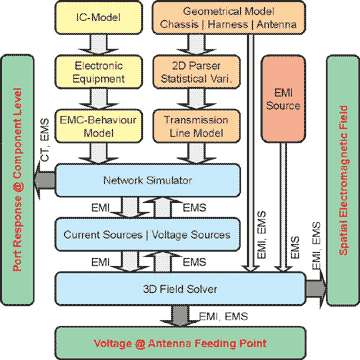
respectively, into the complete car model. Fig. 1 depicts the
proposed EMC simulation strategy, starting from chip level EMC
design up to system level EMC analysis, as applied in the car
development process. The concurrent approach is employed continuously
at all stages in the design flow, from the initial idea up to
the prototyping and the production phase.
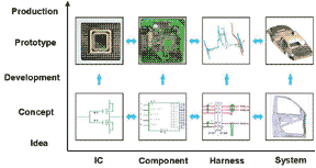 |
| Fig. 1. Concurrent engineering approach
in EMC design. |
Besides the use of the explained multi-level strategy, the described
simulation process enables the continuous exchange of models and
simulation results in both directions, e.g. IC models from IC
manufacturer to the electronic supplier and the car manufacturer
but also chassis or antenna models from the car manufacturer to
the electronic supplier and IC manufacturer. For this reason,
the validation of new concepts can be performed at earlier stages
of the development process and additional measures to fulfill
the EMC standards or to reject system malfunctions can be implemented
in time. This way, the time to market for new electronic products
(not only in the car industry) will be reduced and the reliability
of the system can be improved.
3. Subsystem Modeling
The simulation process presented in the prior section is based
on the multi-level modeling approach and on the exchange of EMC
behavior models. This Section discusses the different subsystem
models used for IC, control module and vehicle. In parallel, the
different modeling techniques applied in the quoted multi-level
modeling approach are explained in detail.
3.1 Active components
Regarding active components used in modern electronics, micro-controller
chips (µC) and bus drivers (e.g. CAN) are of primary interest
in EMC design in automotive industry. Thereof only the mains-borne
disturbance through supply lines from the µC and conducted
emission through output ports from the bus-driver are modeled.
Evaluating an accurate EMC behavior model for all pins of an active
component (including the radiated coupling) would blast the simulation
process.
In order to generate pre-mentioned EMC behavior models, different
modeling techniques can be applied. One commonly used standard
in chip industry is IBIS (Input/Output Buffer Information Specification)
[7]. The IBIS-standard is based on measurements and/or transistor
level simulations of static and dynamic characteristics of the
IC. Additionally, IBIS files include package data (R, L, C), driver
capacitances and clamping diodes behavior. A complete IC contains
different models, depending on the number of different types of
drivers and receivers of the device. Yet it allows no insight
into the actual design, but describes the EMC behavior on the
circuit I/O-terminals. From the circuit information in IBIS format
an electrical circuit model in SPICE syntax is generated as described
in [8, 9].
Guidelines for the extraction of an EMC model describing the conducted
emissions through power-supply lines are presented in [10, 11].
The core model consists of a current generator modeling the main
source of parasitic emissions. The current shape is either extracted
from standardized measurements or computed by means of simulation
tools. Further, the model takes into account first order effects
due to package parasitics and on-chip capacitance, and second
order effects caused by die capacitance, bonding and die connection
inductance. If requested the core coupling to the I/O pins of
the chip can be included in the model.
Both model formulations, IBIS and integrated circuit electromagnetic
models (ICEM), are given as electrical circuit networks in SPICE
syntax. Hence, the requested integration into most of the network
simulators is easily possible.
Additional modeling methods are presented in [12] and [13]. The
first approach is based on the identification of black-box nonlinear
dynamic models. It is suitable for characterizing poorly documented
devices from standard input/output transient measurements. The
latter approach proposes a model for the µC-core based on
supply-current and impedance measurements.
 |
|
Fig. 2. 3D
models for (a) chassis, (b) harness, and (c) rear window
antenna.
|
3.2 Interconnects and passive components
at PCB level
Passive components are characterized satisfactorily in most cases
by the corresponding high frequency models. Of particular interest
however is the modeling of interconnects. Depending on the highest
operating frequency, signal rise times and the nature of structure,
interconnects can be represented by lumped, distributed, or full-wave
models [14]. Lumped RLC-circuit models are used for electrical
short interconnects only, whereas distributed transmissions line
(TL) models described by Telegrapher's equations are applied at
higher switching speeds. The distributed R, L, C, G per unit length
parameters can also take into account frequency-dependent effects
(e.g. skin effect). Spatial EM effects are successfully accomplished
using partial element equivalent circuit (PEEC) models [15]. The
PEEC models are coupled RLC-circuits extracted from the geometry
using the quasi-static or the full-wave solution of Maxwell's
equations.
Concerning the multi-level strategy, the generated models for
each control model are incorporated in the network simulator environment.
 |
|
Fig. 3. Statistical
variations of the transmission and crosstalk parameters
of a 9-wire harness due to mutual position of wires.
|
 |
|
Fig. 4. Recursive harness modeling
process incorporating geometrical data and statistical bundling
variations.
|
3.3 Chassis
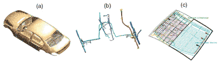
The geometry extraction process starts with the meshing of the
car body. Very detailed geometry data of the car body is available
from the CAD-framework of the car manufacturer. However, with
respect to EMC analysis it is an important task to simplify the
detailed geometry data to a computable mesh without loss of essential
information, and to translate the data into an interchangeable
format for field solvers. To complete the geometrical model, the
centerlines of the interesting harness sections and antenna are
extracted from the CAD-framework and added to the 3D mesh. Fig.
2 exemplifies obtained geometrical models for (a) chassis, (b)
harness, and (c) antenna. The generated geometrical models are
also used for the 3D electromagnetic field calculations (described
in Section 4).
3.4 Cable harness
One major problem encountered in numerical analysis
of high frequency electromagnetic interference in automobiles
is the high complexity of chassis and harness. The harness with
its overall wire length of several kilometers, its small cross-section
diameter compared to its length and its tolerances in geometry
and electrical parameters, limits the accuracy of the EMC simulation.
Likewise, statistical variations need to be considered when generating
the harness model, since the mutual positions of the wires inside
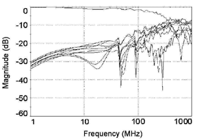
the bundle vary within certain limits. Fig. 3 demonstrates the
influence of the mutual positions of the wires by means of comparison
of far end transmission and crosstalk of a generic harness [16].
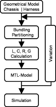
The complexity of the problem can be accomplished by applying
a recursive modeling process as outlined in Fig. 4. In a first
step, the centerline polygon of the geometrical model of the harness
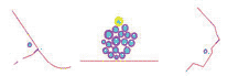
is separated in different segments. Thereafter, the cross-sections
of these segments consisting of the center point of the polygon
and its surrounding chassis shapes are mapped in 2D coordinates.
Some sample sections are plotted in Fig. 5.
Next, the wires inside the automotive harness are positioned statistically
around the 2D center point of each cross-section. Using the 2D
coordinates and the statistical data as input, the TL parameter
matrices R, L, G, C of the harness are calculated for each section.
The obtained multi transmission line model (MTL) is employed to
calculate the current distribution along the wires. This process
is repeated with statistically repositioned wires. Out of the
simulation results a characteristic current distribution is incorporated
in the harness model by means of equivalent current sources for
further calculations.
 |
| Fig. 5. 2D model of harness for TL
parameter extraction. |
3.5 Antenna
One particular application of the EMC simulation in automobiles
is to calculate the voltage at the base of the car antenna caused
by the signal and power transmission via the harness. For this
purpose, the frequency-domain transfer function representing the
coupling from the investigated ports of the harness towards the
antenna is calculated. This transfer function is computed by means
of a 3D field solver with the geometrical models of chassis, harness
and antenna as inputs.
Fig. 6a depicts a practical example where the coupling of a harness
located above the hatrack towards the rear window antenna of the
car is investigated. The calculated transfer function given by
the corresponding scattering parameters is plotted in Fig. 6.
For the frequency-domain simulation the tabulated data of the
coupling is directly incorporated in the multi-level simulation
process. In case of performing a transient analysis an equivalent
circuit model is generated from the scattering parameter data
and integrated in the network simulator as described in [17].
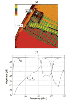 |
| Fig. 6. Harness-antenna-coupling:
(a) geometrical model (b) scattering parameters. |
4. System Simulation
Whereas in previous sections different modeling approaches for
individual subsystems in automotive applications were presented,
this section discusses the system-level simulation of automotive
EMC problems. It focuses on the numerical prediction of the major
EMC challenges in automotive applications: crosstalk, emission,
and immunity. In the following, specific simulation strategies
for the different phenomena are proposed. All strategies are summarized
in Fig. 7.
 |
| Fig. 7. Simulation flow for Crosstalk
(CT), Emission (EMI) and Immunity (EMS). |
4.1 Crosstalk
As partly described in Chapter 3.4 the crosstalk simulation is
based on a MTL model, statistical variations of the bundle, and
terminations at the ports of the harness. The latter are modeled
by the corresponding equipment models consisting of IC models
and circuit models of passive components and interconnects. Connecting
the MTL model to the EMC behavior models for the equipment the
crosstalk simulation can be performed (compare Fig. 7). In case
of linear loads the joined model is analyzed in frequency-domain
with TL simulators. For non-linear terminations network simulators
that support MTL models are employed to calculate the time-domain
solution.
For the purpose of illustration the crosstalk occurring in four
twisted pair cables is investigated [16]. The twisted pairs are
excited by simultaneously switched PWM-signals. Applying the modeling
procedure described in Fig. 4 and performing the simulation process
outlined in Fig. 8 the crosstalk for ten statistical positioned
wire bundles is calculated.
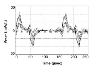 |
| Fig. 8. Crosstalk simulation: Transient
port response using ten different wire bundles. |
4.2 Emission
The calculation of EMI starts again with the generation of the
subsystem models for chassis, harness and equipment. Thereafter,
the harness and equipment models are joined together and the current
distribution along the wires of the harness is calculated using
a network solver and TL models. The obtained current distribution
is implemented as impressed current sources (Huygen's principle)
in the meshed space or surface of the geometrical model for the
harness defined for the field solver. In the final step, the geometrical
models for chassis and the impressed current sources are imported
to a 3D field solver and the radiation from the harness is calculated.
Fig. 9a illustrates the EM field in a cut plane during this 3D
radiation.
Rather than the 3D fields, in many practical applications the
voltage obtained at the antenna feeding point (e.g. located in
the rear window) is of particular interest [18]. The incorporation
of the antenna model into the car environment is described in
Chapter 3.5. At this point, the system configuration depicted
in Fig. 6 is excited with a non-linear driver at port 1 (harness).
The calculated transient response is plotted in Fig. 9.
4.3 Immunity
For EMS analysis, basically the reversed simulation process than
for EMI is applied. First, using the geometrical model of the
chassis a 3D field solver is employed to calculate the electromagnetic
field within the car body caused by the EMI source. The obtained
E- and H-field is analyzed at the position of the harness, and
the corresponding current and voltage values are calculated. Next,
the currents and voltages are impressed as distributed controlled
sources in the TL network [19]. Finally, the obtained electrical
circuit including the equipment models is imported in the network
simulator and the port response is simulated.
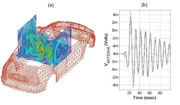 |
| Fig. 9. Emission simulation: (a)
electromagnetic field (b) voltage at the antenna feeding point. |
5. Validation
To prove the feasibility of the proposed continuous concurrent
EMC simulation process, EMC measurements need to be performed
simultaneously. The validation is carried out at the different
partners (IC manufacturer, electronic supplier, car manufacturer)
contributing to the vehicle design. As a result of the validation
the simulation process can be improved perpetually. Nevertheless,
EMC simulations will not replace EMC measurements and EMC standards.
Both still play an important role to guarantee the quality and
functionality of the final product. However, the proposed simulation
process provides a useful tool for the evaluation of new concepts
regarding their EMC characteristics at an earlier stage of the
design process.
6. Conclusion
In recent years, most innovations in the automotive industry are
accompanied by new electronics. In consequence of the growing
number of electrical equipment the electromagnetic noise level
is rising in automobiles. The increased electromagnetic emissions
place high demands on the EMC engineer to fulfill requested EMC
standards and guarantee the functional integrity of the electronic
systems. The early detection and rejection of potential EMC problems
becomes mandatory for the success of new technologies.
This paper presented a continuous concurrent EMC modeling and
simulation process for automotive applications. Essential guidelines
for the generation of EMC behavior models of components and structures
from IC designer, electronic supplier and car manufacturer involved
in the design were proposed. Furthermore, specific simulation
strategies for the different phenomena crosstalk, emission, and
immunity were discussed.
Employing EMC simulation, the goal of early design-concept validation
and on-time implementation of EMC measures can be achieved. Although
EMC simulation will not replace the validation of the final design
by measurements, it reduces the risk of EMC failure and aids a
scheduled launch of new products.
Acknowledgement
This work was supported by the European Commission under contract
number G3RD-2000-00305.
References
1. I. E. Noble, "Electromagnetic Compatibility in the Automotive
Environment," in IEE Proc. Science, Measurements and Technology,
vol. 14(4), 1994, pp. 252-258.
2. J.C. Kedzia. "Numerical EMC in Ground Transportation:
How to Manage Efficiently Realistic Automotive Problems,"
in Proc. PAM Users Conference in Asia - PUCA'99, Nov. 1999.
3. J. C. Rautio, "MIC Simulation Column - A Standard Stripline
Benchmark," Int. Journal of Microwave & Millimeter-Wave
Computer-Aided Engineering, vol. 4, no. 2, April 1994, pp. 209-212.
4. A. Englmaier, "Methods and Models for EMC-Simulation,"
PhD Thesis, Technical University Munich, June 1998.
5. F. Canavera, J.C. Kedzaia, P. Ravier, B. Scholl, "Numerical
Simulation for Early EMC Design of Cars," in Proc. CEM 2000
Symposium, Brugge, Sept. 2000.
6. B. Scholl, "Automotive EMC Problems & Research,"
in Proc. AutoEMC Workshop, Paris, France, June 2000.
7. IBIS I/O Buffer Information Specification, URL: https://www.eigroup.org/ibis/ibis.htm.
8. F. Haslinger, B. Unger, M. Maurer, M. Tröscher, R. Weigel,
"EMC Modeling of Nonlinear Components for Automotive Applications,"
in Proc. 14th Int. Zurich Symp. on EMC, Zurich, Switzerland, Feb.
2001.
9. I. A. Maio, I. S. Stievano, F. G. Canavero, "Signal Integrity
and Behavioral Models of Digital Devices," in Proc. 13th
Int. Zurich Symp. on EMC, Zurich, Switzerland, Feb. 1999.
10. S. Baffreu, C. Huet, C. Marot, S. Calvet, E. Sicard, "A
Standard Model For Prediction The Parasitic Emission of Micro-Controllers,"
in Proc. EMC Europe 2002, Sorrento, Italy, Sept. 2002, pp. 481ff.
11. ---, "Cookbook for Integrated Circuit Electromagnetic
Model (ICEM)", Release 1.d, Oct. 2001, URL: www.ute-fr.com.
12. F. Canavero, I. A. Maio, I. S. Stievano, "Black-Box Models
of Digital IC Ports for EMC Simulations," in Proc. 14th Int.
Zurich Symp. EMC, Zurich, Switzerland, February 2001.
13. J. Held, B. Unger, L. Girardeau, "Measurement of the
Supply-Current and Internal Impedance of VLSIs in a wide Frequency
Range," Int. Symp. on EMC 2003, Istanbul, Turkey, May 2003.
14. Achar, R., Nackla, M. S., "Simulation of High-Speed Interconnects",
IEEE Proceedings, vol. 89. no. 5, May 2001, pp. 693-727.
15. A. Ruehli, "Equivalent Circuit Models for Three-Dimensional
Multiconductor Systems," IEEE Trans. Microwave Theory and
Techniques, vol. 22, no. 3, March 1974, pp. 216-221.
16. A. Englmaier, B. Scholl, "EMC Modelling Strategy For
Automotive Applications," Int. SimLab User Conference 2000,
Munich, Nov 2000.
17. R. Neumayer, A. Stelzer, F. Haslinger, R. Weigel, "On
the Synthesis of Equivalent Circuit Models for Multiports Characterized
by Frequency-Dependent Parameters", IEEE Trans. Microwave
Theory and Techniques, vol. 50, Dec. 2002.
18. B. Scholl, W. Kühn, P. Malnoult, H. Luzet, J.C. Kedzia.
"Electromagnetic Interferences, Conducted and Radiated Emissions
of a Harness towards a Receiving Antenna: Comparison of Numerical
Results with Measurements," in Proc. Euro-PAM'98 Conference,
Tours, France, Oct. 1998.
19. A. C. Cangellaris, "Distributed Equivalent Sources for
the Analysis of Multiconductor Transmission Line Exited by an
Electromagnetic Field", IEEE Transactions on Microwave Theory
and Technique, vol. 36, no. 10, Oct. 1988, pp. 1445-1448.
 Roland
Neumayer (S'01) received the M.S. degree from Loughborough
University, England, UK, and the Diploma degree from Johannes
Kepler University, Linz, Austria, both in mechatronics, in 1999,
and 2000, respectively. He is working towards the Ph.D. degree
in the department of communications and information engineering
at Johannes Kepler University, Linz. Currently, he is engaged
with the European research project for continuous simulation of
EMC in automotive applications (COSIME). His research interests
include network synthesis, modeling and simulation techniques
for EMC analysis. Roland
Neumayer (S'01) received the M.S. degree from Loughborough
University, England, UK, and the Diploma degree from Johannes
Kepler University, Linz, Austria, both in mechatronics, in 1999,
and 2000, respectively. He is working towards the Ph.D. degree
in the department of communications and information engineering
at Johannes Kepler University, Linz. Currently, he is engaged
with the European research project for continuous simulation of
EMC in automotive applications (COSIME). His research interests
include network synthesis, modeling and simulation techniques
for EMC analysis.
 Andreas
Stelzer (M'00) received the Diploma Engineer degree in electrical
engineering from the Technical University of Vienna, Austria,
in 1994. In 2000, he received the Dr.techn. degree in mechatronics
with honors sub auspiciis praesidentis rei publicae from the Johannes
Kepler University. Since 2000 he is with the Institute for Communications
and Information Engineering. His research work focuses on microwave
sensors for industrial applications, RF- and microwave subsystems,
EMC modeling, DSP and micro controller boards as well as high
resolution evaluation algorithms for sensor signals. Andreas
Stelzer (M'00) received the Diploma Engineer degree in electrical
engineering from the Technical University of Vienna, Austria,
in 1994. In 2000, he received the Dr.techn. degree in mechatronics
with honors sub auspiciis praesidentis rei publicae from the Johannes
Kepler University. Since 2000 he is with the Institute for Communications
and Information Engineering. His research work focuses on microwave
sensors for industrial applications, RF- and microwave subsystems,
EMC modeling, DSP and micro controller boards as well as high
resolution evaluation algorithms for sensor signals.
 Friedrich
Haslinger received the Dr.techn. degree in mechatronics from
the Johannes Kepler University in Linz, Austria in 2001. Mr. Haslinger
then joined the BMW Group in Munich, Germany, where he is engaged
with electromagnetic compatibility in cars. His main interests
are various aspects of simulation of electromagnetic compatibility
effects, especially the integration of non-linear noise sources. Friedrich
Haslinger received the Dr.techn. degree in mechatronics from
the Johannes Kepler University in Linz, Austria in 2001. Mr. Haslinger
then joined the BMW Group in Munich, Germany, where he is engaged
with electromagnetic compatibility in cars. His main interests
are various aspects of simulation of electromagnetic compatibility
effects, especially the integration of non-linear noise sources.
 Gernot
Steinmair (S'01) received the M.S. degree from Loughborough
University, England, UK, and the Diploma degree from Johannes
Kepler University, Linz, Austria, both in mechatronics, in 1999,
and 2000, respectively. He is working towards the Ph.D. degree
at the department of communications and information engineering
at Johannes Kepler University, Linz. Currently, he is engaged
with the department for electromagnetic compatibility of Bayrische
Motorenwerke (BMW AG), Munich, Germany. His research interests
include EMC modeling, model order reduction and simulation techniques
for EMC analysis. Gernot
Steinmair (S'01) received the M.S. degree from Loughborough
University, England, UK, and the Diploma degree from Johannes
Kepler University, Linz, Austria, both in mechatronics, in 1999,
and 2000, respectively. He is working towards the Ph.D. degree
at the department of communications and information engineering
at Johannes Kepler University, Linz. Currently, he is engaged
with the department for electromagnetic compatibility of Bayrische
Motorenwerke (BMW AG), Munich, Germany. His research interests
include EMC modeling, model order reduction and simulation techniques
for EMC analysis.
 Matthias
Troescher received a Diploma in physics from the Technical
University Munich, Germany, in 1994 and a Ph.D. degree in the
Doctoral Program of Engineering Sciences from the Johannes Kepler
University Linz, Austria, in 2000. From 1991 to 1994 he assisted
in a European project for EMC simulation at the Fraunhofer Institute
for Solid State Technology in Munich, Germany. In 1994 and 1995,
he worked with the Institute for Radiation Protection in Munich,
following which he joined the research department of BMW AG Munich.
He joined SimLab Software GmbH (Munich) in 1999, where he is responsible
for publications, technical support and product development. Matthias
Troescher received a Diploma in physics from the Technical
University Munich, Germany, in 1994 and a Ph.D. degree in the
Doctoral Program of Engineering Sciences from the Johannes Kepler
University Linz, Austria, in 2000. From 1991 to 1994 he assisted
in a European project for EMC simulation at the Fraunhofer Institute
for Solid State Technology in Munich, Germany. In 1994 and 1995,
he worked with the Institute for Radiation Protection in Munich,
following which he joined the research department of BMW AG Munich.
He joined SimLab Software GmbH (Munich) in 1999, where he is responsible
for publications, technical support and product development.
 Joachim
Held was born in 1960 in Germany. He graduated in 1986 in
electrical engineering at the Technical University of Erlangen,
Germany. 1996 he joined the Siemens AG delivering EMC-support,
where he works on innovative principles of inductive current dividing
for supply-systems, and special measurement-methods for VLSI supply-currents. Joachim
Held was born in 1960 in Germany. He graduated in 1986 in
electrical engineering at the Technical University of Erlangen,
Germany. 1996 he joined the Siemens AG delivering EMC-support,
where he works on innovative principles of inductive current dividing
for supply-systems, and special measurement-methods for VLSI supply-currents.
 Bernhard
Unger was born in 1940 in Germany. After studies of physics
and graduation he joined Siemens AG in 1972. In the first years
he was mainly concerned with ECL-gate array development. Presently
he is working on Signal Integrity and EMI issues. Bernhard
Unger was born in 1940 in Germany. After studies of physics
and graduation he joined Siemens AG in 1972. In the first years
he was mainly concerned with ECL-gate array development. Presently
he is working on Signal Integrity and EMI issues.
 Robert
Weigel (F'01) received the Dr.-Ing. and the Dr.-Ing.habil.
degrees, both in electrical engineering and computer science,
from the Munich University of Technology in Germany, in 1989 and
1992, respectively. From 1994 to 1996 he was a Professor for RF
Circuits and Systems at the Munich University of Technology. Since
1996, he has been Director of the Institute for Communications
and Information Engineering at the University of Linz, Austria.
In August 1999, he co-founded DICE - Danube Integrated Circuit
Engineering, Linz, meanwhile an Infineon Technologies Development
Center, which is devoted to the design of mobile radio circuits
and systems. In 2000, he has been appointed a Professor for RF
Engineering at the Tongji University in Shanghai, China. In 2002,
he moved to Erlangen, Germany, to accept the Directorship of the
Institute for Technical Electronics at the University of Erlangen-Nuremberg.
EMC Robert
Weigel (F'01) received the Dr.-Ing. and the Dr.-Ing.habil.
degrees, both in electrical engineering and computer science,
from the Munich University of Technology in Germany, in 1989 and
1992, respectively. From 1994 to 1996 he was a Professor for RF
Circuits and Systems at the Munich University of Technology. Since
1996, he has been Director of the Institute for Communications
and Information Engineering at the University of Linz, Austria.
In August 1999, he co-founded DICE - Danube Integrated Circuit
Engineering, Linz, meanwhile an Infineon Technologies Development
Center, which is devoted to the design of mobile radio circuits
and systems. In 2000, he has been appointed a Professor for RF
Engineering at the Tongji University in Shanghai, China. In 2002,
he moved to Erlangen, Germany, to accept the Directorship of the
Institute for Technical Electronics at the University of Erlangen-Nuremberg.
EMC
|
|
|