Invited Speakers

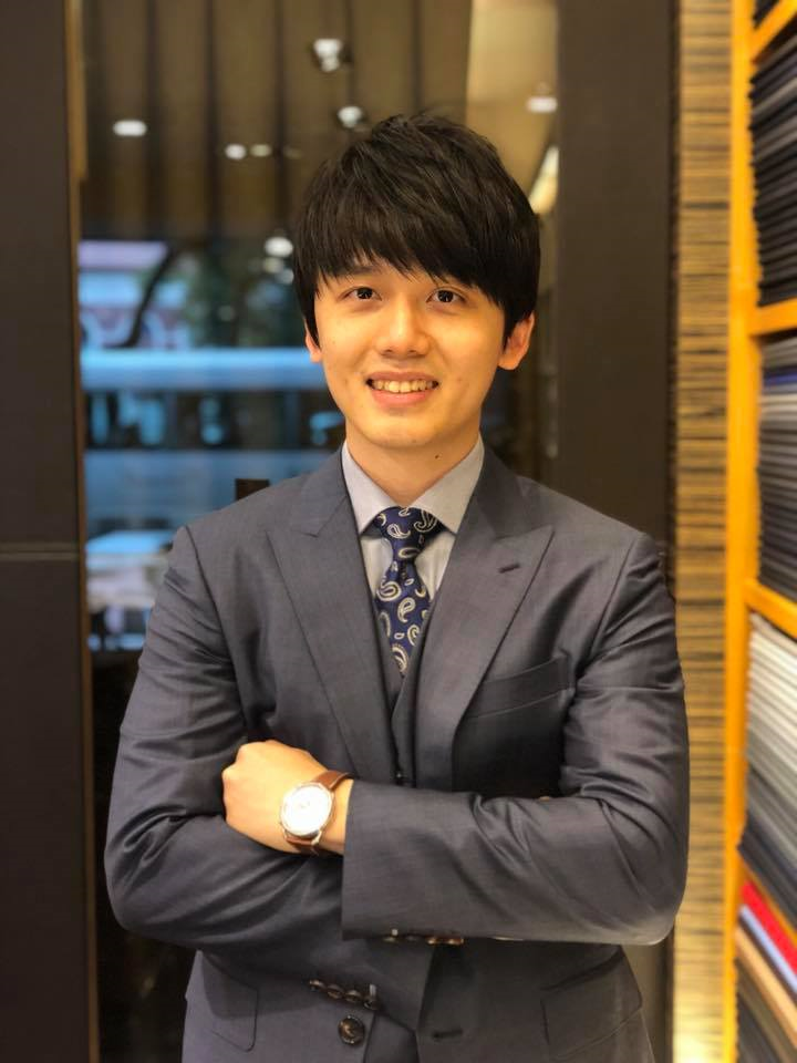
CHEN, LI (HARDY)
Process Control Solution, KLA-Tencor
Title: Yield Challenges and Innovative Inspection & Metrology Solutions for 10nm and beyond
Abstract: Computational simulations offer a cost-effective way to peek into future challenges in wafer manufacturing. In this paper, a variety of simulation methods will be discussed, including their ability to better predict process changes and the implications to inspection and metrology. Process simulation software Coventor SEMulator3D® was used to visualize process variations and an in-house rigorous coupled-wave analysis (RCWA) engine was built to calculate the propagation of E-field through wafer topology [1]. By simulating a self-aligned gate contact and via process, we estimate the process window, defects-of-interest, and metrology requirements. Another study estimates the yield impact of film particles being decorated through different process steps. The final series of work attempts to understand the responses of inspection tools to varied defect and pitch sizes on an extreme ultraviolet lithography (EUV) line and space pattern. As a semiconductor equipment manufacturer, KLA-Tencor values the detail provided by these simulations as they highlight potential yield challenges, which guides our development of next-generation process control solutions [2,3].
Biography: Li Chen received B.S degree in Physics in Taiwan National Central University and M.S degree in Material Science and Engineering from Northwestern University in Illinois, United States. He joined KLA-Tencor, Taiwan in 2011 working as applications engineer specializing in wafer defect inspection, supporting inline monitoring of process defects in 2x and 1x nm logic device technology node. He is currently involved in Process Control Solutions division of KLA-Tencor’s Global Customer Solutions group and recently he is engaging himself in the simulations-guided methodology to investigate advance manufacturing yield issues and providing process control solutions to meet sub-10nm challenges.