Invited Speaker

Hafnia-Based Ferroelectric Devices for Lower Power Memory and AI Applications
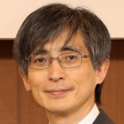
Shinichi Takagi (The University of Tokyo)
Biography:Shinichi Takagi was born in Tokyo, Japan, on August 25, 1959. He received the B.S., M.S. and Ph.D. degrees in electronic engineering from the University of Tokyo, Tokyo, Japan, in 1982, 1984, and 1987, respectively. He joined the Toshiba Research and Development Center, Kawasaki, Japan, in 1987, where he has been engaged in the research on the device physics of Si MOSFETs, including the carrier transport in the inversion layer, the impact ionization phenomena, the hot carrier degradation and the electric properties of Si/SiO2 interface. From 1993 to 1995, he was a Visiting Scholar at Stanford University, Stanford, CA, where he studied the Si/SiGe hetero-structure devices. Since returning to the ULSI Research Laboratories, he was also engaged in the physics and technology of the reliability of SiO2, ferroelectric devices, and strained-Si MOS devices. He worked for the MIRAI Project as the leader of Ultra-High Performance New Transistor Structures Theme from 2001 to 2007. In October 2003, he moved to the University of Tokyo, where he is currently working as a professor in the department of Electrical Engineering and Information Systems, School of Engineering. His recent interests include the science and the technologies of advanced CMOS devices using Ge and III-Vs, tunneling FETs, and ferroelectric devices. Dr. Takagi served on the technical program committee on several international conferences including International Electron Device Meeting, Symposium on VLSI Technology, International Reliability Physics Symposium, International Conference on Solid State Device and Materials, and International Solid State Circuits Conference. He is a member of the IEEE Electron Device Society and the Japan Society of Applied Physics.