Invited Speaker

Flip Chip Joining with Injection Molded Solder Technology
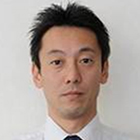
Takashi Hisada (IBM)
Biography: Dr. Takashi Hisada is a member of the IBM Academy of Technology and the manager of the Neuromorphic Interconnection group in IBM Research - Tokyo. After receiving his BS in physics from Osaka University, he joined IBM in 1992 where he started his career as an engineer developing semiconductor packages. He developed a fine pitch wire bonding process for ASIC products, a robust packaging process for low-k/ultra low-k wafers, and so on, From 2006 to 2015, he led the package development team responsible for developing the packaging process, package design, qualifications for the technologies and products. In 2014, he earned his PhD in Materials and Manufacturing Science at Osaka University. Since joining IBM Research - Tokyo in 2015, he has been leading the research and development of ultra-high-density chip carriers and ultra-fine-pitch chip joining for neuromorphic devices. Currently he is the chair of Technical Committee 6 - High Density Substrate in IEEE EPS.