|
 |
|
|

Technical
Seminar |
|
|
|
|
|
Integrated Circuit Intrinsic Reliability
|
|
|
DATE/TIME
Wednesday, February 16, 2005 (5:30pm to 7:30pm)
|
|
PLACE
Physiology Bldg. Room 243 (2nd floor) (CSU, Fort Collins, CO)
|
|
DIRECTIONS
|
-
To
Colorado State University
-
To
Physiology Building (note change from Physiology 103 to Physiology
243)
-
Physiology
Building is on the south side of campus, at the NE corner of Centre
Avenue and Lake Street. From I-25, it is easiest to take
Prospect Road westbound. After passing College Avenue, turn
right onto Centre Avenue and park at parking lot on right side of road
before reaching Lake Street.
-
Park south of
Physiology Building -- free after 4pm
|
|
COST
Free. As always, pizza &
drinks will be provided. |
|
|
ABSTRACT The
scaling of silicon integrated circuits to the deep submicron realm has
presented challenges to maintaining the long-term reliability of these
devices.
In the past, the wearout mechanisms of silicon devices typically
began long after the useful life of the product was over.
With the scaling down of both the transistors and the
metallization, the onset of wearout is becoming increasingly close to the
expected life of the product.
The integrated circuit wearout mechanisms discussed are hot carrier
injection (HCI) gate oxide wearout, negative bias temperature instability
(NBTI), electromigration, and stress migration.
HCI and NBTI cause changes in parameters (such as Vt, Gm, and drain
current) of individual transistors.
The others can cause changes in circuit characteristics or
catastrophic circuit failure, such as a short or open.
This presentation discusses the causes of the wearout phenomenon,
its effect on the individual transistor and possible effects on the
circuit, and how it is measured.
It then discusses steps a designer can take to account for device
degradation and mitigate its effect. |
|
PRESENTATION SLIDES
pdf
|
|
|
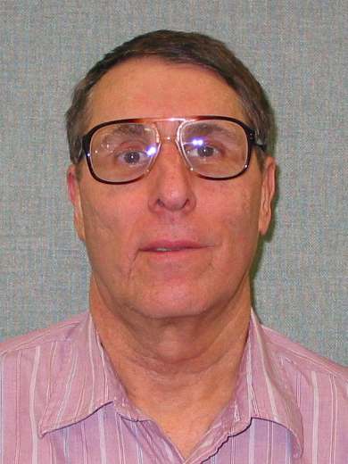
DR. DENNIS
EATON
(Agilent
Technologies, Fort Collins, CO)
|
|
Dennis Eaton received the BS degree in
physics from Harvey Mudd College, Claremont,CA, and the MS and PhD
degrees in physics from the University of Illinois, Urbana-Champaign, IL.
He then joined Bell Labs where he worked on bipolar integrated
circuits and metallization. In
1976, Dr. Eaton joined Hewlett-Packard Company, working in MOS technology
and processing. He later held
management positions in silicon process development and manufacturing.
Since 1984, Dr. Eaton has held engineering and management positions
in semiconductor device and product reliability at Hewlett-Packard and
Agilent Technologies. He has
been responsible for reliability testing, device reliability, and
reliability estimation. He
has authored papers on process technology, process control, and
reliability. Dr. Eaton is a
member of IEEE and the American Society for Quality (ASQ). He is a
Certified Reliability Engineer of the ASQ. |
|
|
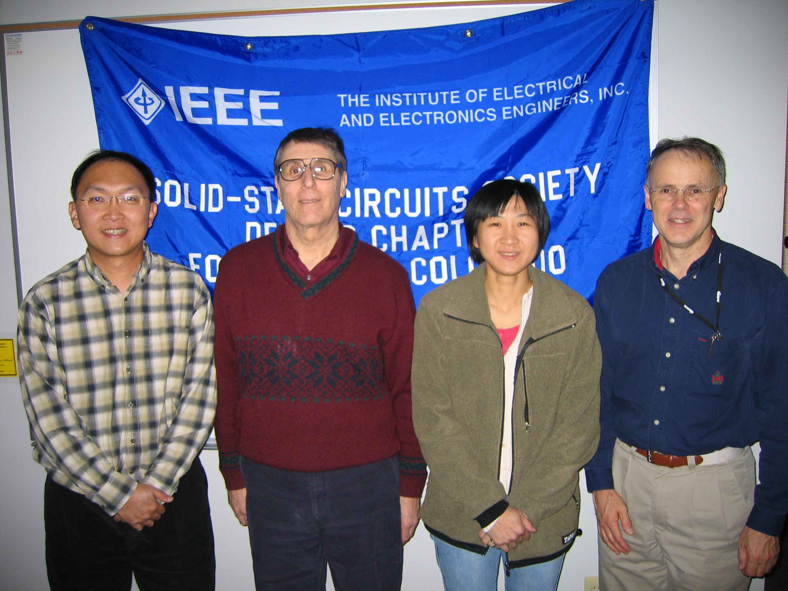
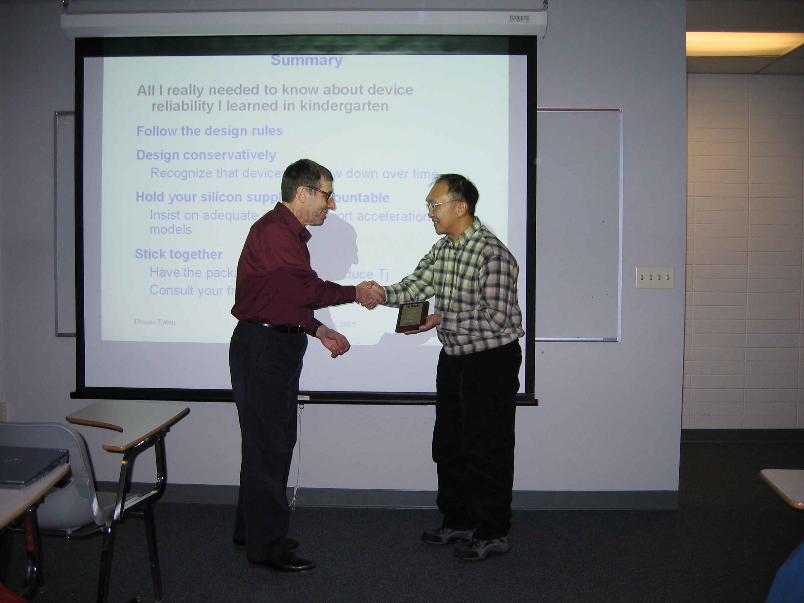
PHOTOS
Courtesy of Bob Barnes & Don Morris
|
|
|