|
 |
|
|

Technical
Seminar |
|
|
|
|
|
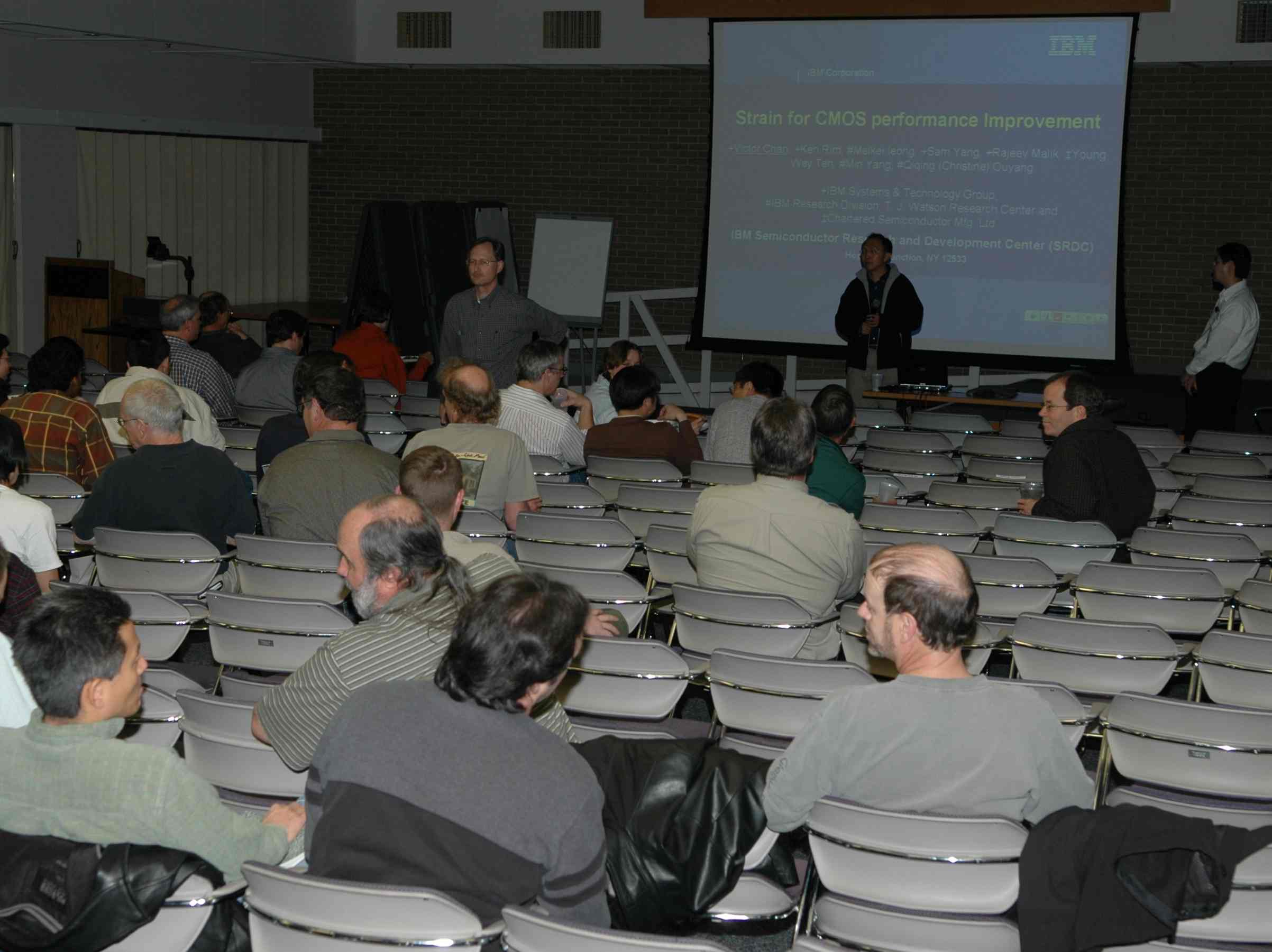
Strain Engineering for CMOS Performance Improvement
|
|
|
DATE/TIME
Friday, January 27, 2006 (4:30-6:00pm)
|
|
PLACE
Bldg. 1 Auditorium (Avago Technologies,
Fort Collins, CO, formerly Agilent Technologies)
|
|
DIRECTIONS
From I-25, take Harmony Road Exit (Exit
265) westbound, and enter Avago/HP/Intel campus on right. Avago/HP/Intel
campus is on the NE corner of Harmony Road and Ziegler Road.
Proceed to Bldg. 1 Lobby to sign-in and meet host for escort to
Auditorium. |
|
Non-Avago/HP
Attendees: Please arrive punctually at 4:15pm as you will need to be
escorted to the seminar room. We appreciate a courtesy RSVP to
bob.barnes@avagotech.com to
expedite sign-in and to help us with a headcount estimate for
food/drinks. |
|
|
ABSTRACT
|
|
Device improvement
with strain engineering is considered a way to enhance the carrier
mobility. Several stress-transfer techniques (such as
etch-stop liner, stress transfer technique, e-SiGe) using extra
integration process into an existing baseline process is
demonstrated. In addition, new preparation techniques of
strained-Si surface (e.g., biaxial tensile stress) and different
substrate orientation to enhance mobility are introduced. The
challenges and vitality of each method will be discussed and
compared. In addition, we will highlight how the stress
oriented from the layout geometry affects the device electrical
behavior. The issues and improvement in the circuit level
device modeling will be discussed. |
|
PRESENTATION SLIDES
presentation
paper (copyright
IEEE) |
|
|
DR. VICTOR
CHAN (IBM, Hopewell Junction, NY)
|
|
Victor W. C. Chan
received the B.E. degree in electrical
engineering from the University of New South Wales, Sydney, Australia,
in 1995, and the Ph.D.E.E. degree from Hong Kong University of Science
and Technology, Hong Kong, in 2001. From 1996 to 1998, he was at
Chartered Semiconductor Manufacturing, Singapore, in the 0.35um & 0.45um
etch process development. Since 2002, he has been with the IBM
System and Technology Group, Microlectronics Divison, Hopewell Junction,
NY, developing leading-edge 90nm and 65nm bulk CMOS technologies to
support IBM's foundry business with local strain engineering, aggressive
channel length and gate oxide reduction. He also worked in 90nm
CMOS SOI technology to improve product performance-limited yield.
The high performance products include Apple G5, game chips such as Sony
playstation and Microsoft XBox. He has also collaborated the IBM T.J.
Watson Research Center, Yorktown Heights, NY, for next generation CMOS
solutions such as mobility enhancement techniques, wafer orientation,
and 3-D integration. |
|
|
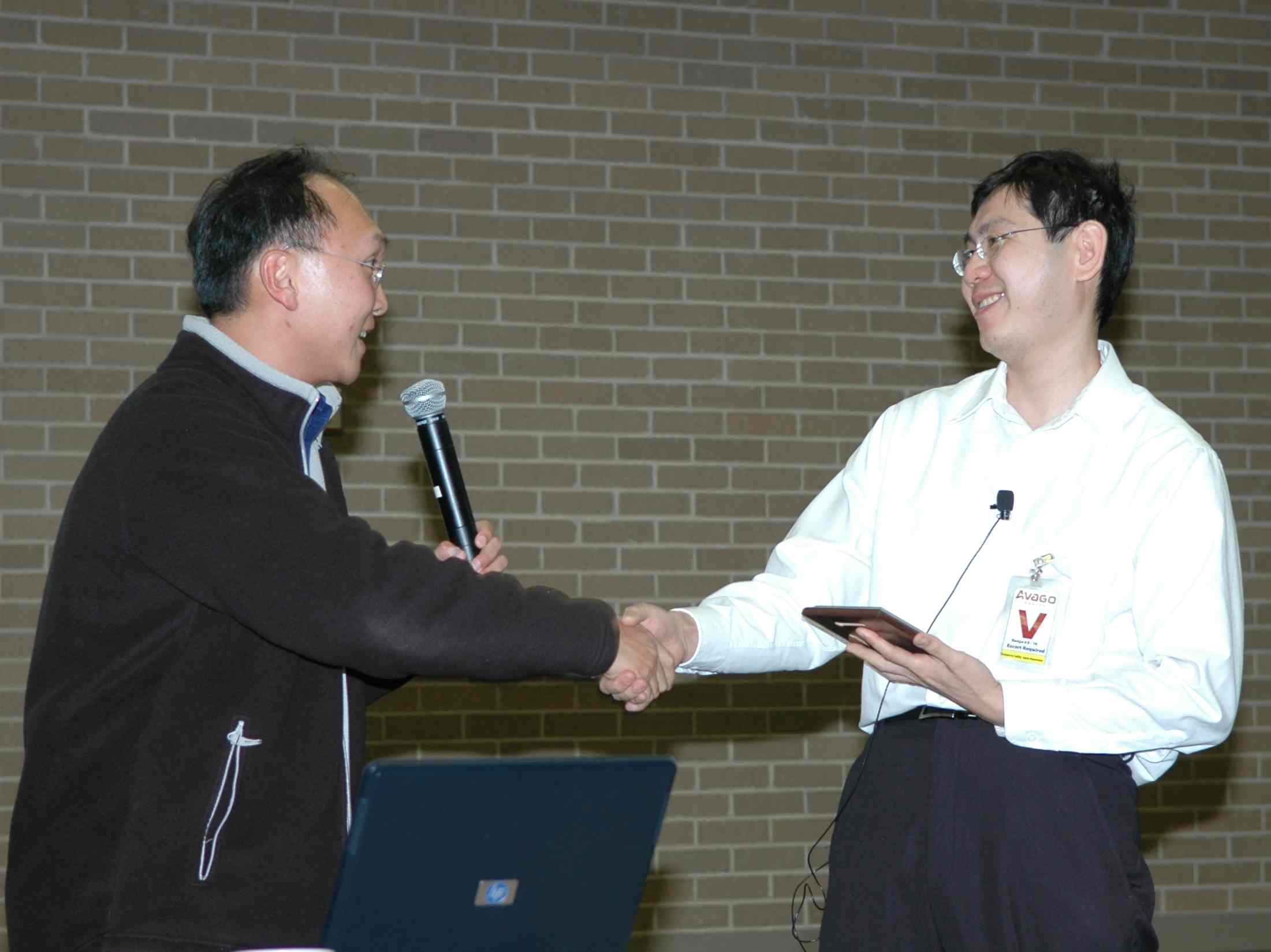
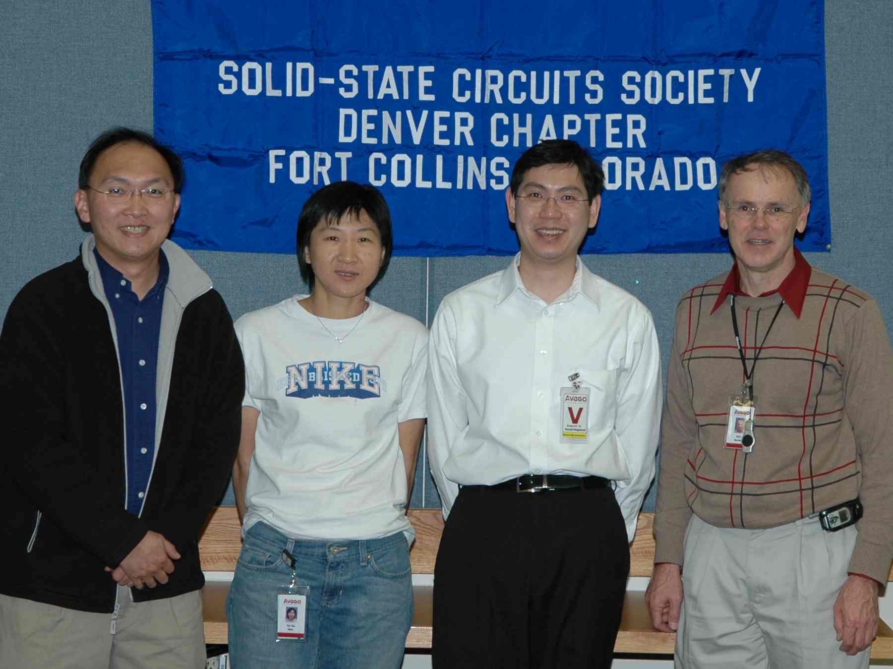
PHOTOS
Courtesy of Bob Barnes
|
 |
 |
 |
|