 |
 |
|

Technical
Seminar
Distinguished Lecturer Series |
 |
 |
|
|
|
Nanometer CMOS: An Analog Challenge |
|
|
DATE/TIME
Thursday, May 11, 2006
(10:00am to 11:30am) NOTE MORNING TIME!!! |
|
PLACE
Bldg. 1 Auditorium (Avago
Technologies, Fort Collins, CO, formerly Agilent Technologies) |
|
DIRECTIONS
|
|
Non-Avago
Attendees: Please arrive punctually at 9:45am as you will
need to be escorted to the seminar
room. RSVP to
bob.barnes@avagotech.com
to expedite sign-in and to help us with a headcount estimate for
food/drinks. |
|
From I-25, take Harmony Road Exit (Exit
265) westbound, and enter Agilent/HP campus on right. Avago/HP/Intel
campus is on the NE corner of Harmony Road and Ziegler Road.
Proceed to Bldg. 1 Lobby to sign-in and meet host for escort to
Auditorium. |
|
COST
Free. As always, food &
drinks will be provided. |
|
|
ABSTRACT
|
|
The
technical evolution in the semiconductor industry has reached a point
where the smallest lateral dimensions have reached the level of tenths
of nanometers. The scaling of the traditional MOS transistor will
still allow continuing on this evolutionary path for some generations.
In this phase of technological development, questions arise around the
economical benefit from scaling and from the inevitable power crisis on
chip. |
|
In this talk,
the attention will be focused on the third existential issue:
variability. More and more physical effects jeopardize the digital
paradigm of clean “ones” and zeros” that separate the mathematical world
of algorithms and software from the execution in the physical domain.
Consequently, more and more analog effects
penetrate into the digital vocabulary. Variability is a rather
loosely defined term, under which a rather wide-spread range of
phenomena are listed. |
|
This talk will
cover mismatch in MOS transistors due to granularity of the doping
charge as well as the problems around substrate noise.
A first
step towards mastering the variability problem is to monitor the
physical parameters in a digital chip. A method will be shown for
measuring various analog parameters in digital cores. |
|
PRESENTATION SLIDES
pdf |
|
REFERENCES
JSSC Classic Paper on MOSFET
Matching |
|
|
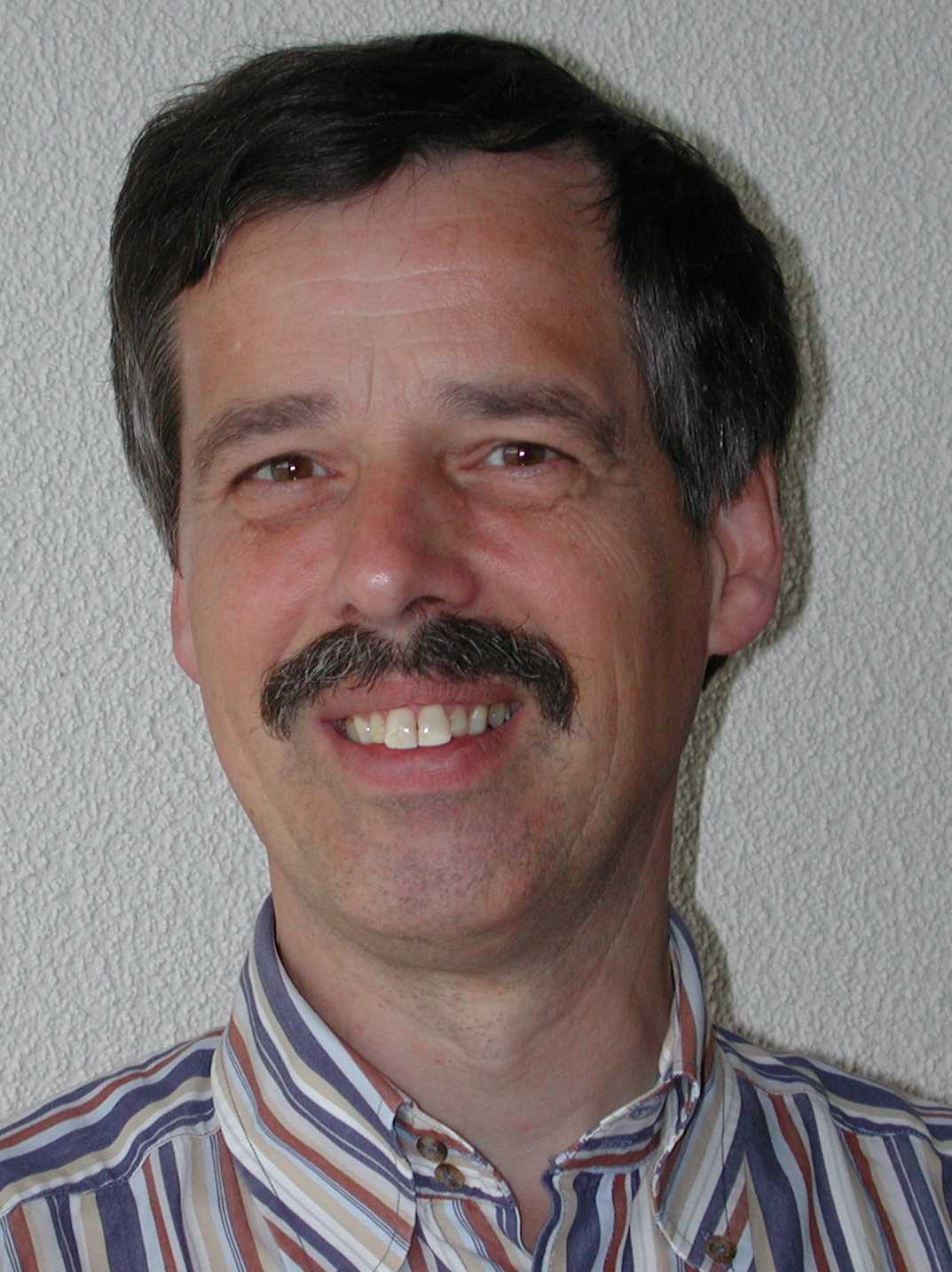
DR. MARCEL PELGROM (Philips Research, Eindhoven, The Netherlands)
|
 |
Marcel Pelgrom (M’82)
received his masters’ degree in electrical engineering at Twente
University in Enschede the Netherlands in 1979, after which he joined
Philips Research Labs. In 1988 he received a PhD from Twente University
on his research work on Charge-Coupled Devices for video applications.
Since then, his research has covered topics as MOS matching properties,
analog-to-digital conversion, digital image correlation, and various
analog building blocks. He has headed several project teams and
was a team leader for high-speed analog-to-digital conversion.
From 1996 to 2003, he was a department head for mixed-signal electronics
in Philips Research. Next to various activities concerning
industry-academic relations, he is presently involved as a research
fellow in research on the edge of design and technology. In 2003,
he spent a sabbatical in Stanford University where he was appointed
Consulting Professor. |
|
Dr. Pelgrom has written over 40
publications, three book chapters, and holds 30 US patents. He
lectures at Twente University, in the Philips training department, and
for MEAD Inc.. His area of specialization is analog-to-digital
conversion, MOS mismatch phenomena, and low-power analog electronics. |
|
|
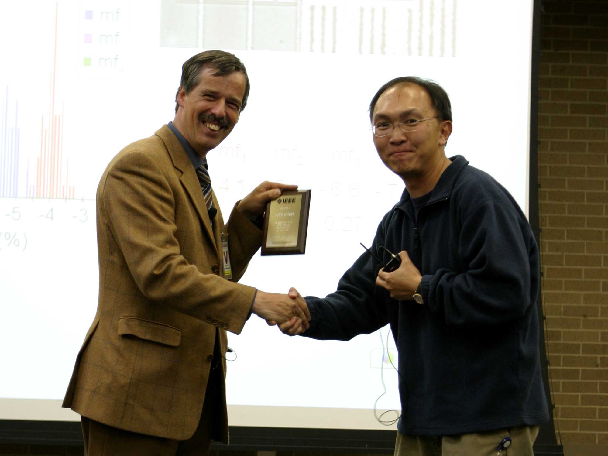
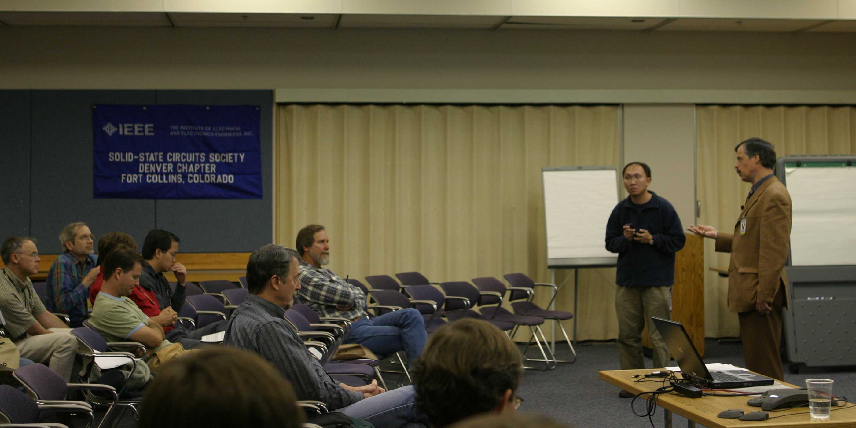
PHOTOS
Courtesy of Tin Tin Wee |
|
 |
|
 |
|
|