In this issue you will find two practical
papers that should interest members of the EMC community.
The first is entitled “When Correlation Lets You Down,
Pre-Compliance Testing Made Usable” by Mathew Aschenberg,
Derrell Gottwald, and Charles Grasso. This paper will provide
assistance to the many of you who have struggled with using
pre-compliance measurements to predict the results of compliance
tests. The second, entitled “Reducing Emissions in the
Buck Converter SMPS,” by Scott Mee and James Teune is
a revised and expanded version of the paper they presented
at the 2002 IEEE International Symposium on EMC in Minneapolis.
It has been reprinted by permission. The paper is a very practical
discussion of how to reduce emissions in these power supplies.
I think you will find the way they relate before and after
emission measurements to circuit measurements is an especially
useful way to quantify the effect of design changes.
The purpose of this section is to disseminate practical information
to the EMC community. In some cases the material is entirely
original. In others, the material is not new but has been
made either more understandable or accessible to the community.
In others, the material has been previously presented at a
conference but has been deemed especially worthy of wider
dissemination. Readers wishing to share such information with
colleagues in the EMC community are encouraged to submit papers
or application notes for this section of the Newsletter. See
page 3 for my e-mail, FAX and real mail address. While all
material will be reviewed prior to acceptance, the criteria
are different from those of Transactions papers. Specifically,
while it is not necessary that the paper be archival, it is
necessary that the paper be useful and of interest to readers
of the Newsletter.
Comments from readers concerning these papers are welcome,
either as a letter (or e-mail) to the Associate Editor or
directly to the authors. |
Getting a GTEM to accurately
mirror the emissions profile measured at our local OATS has been
a real struggle. The test setup has been tinkered, tweaked and cajoled
in a thousand different ways with hopes the goose will lay that
golden egg. With an undersized GTEM, and an over abundance of cables,
correlating the GTEM to an OATS was unattainable.
Site sources produced very repeatable, correlated results to the
OATS, but when attempting to measure a more complex device the repeatability
and correlation evaporates. Correlating measurements of units with
cables is like tackling a greased pig, but that is the real task
many of us face when performing pre-compliance testing. Few of us
design and sell products as simple as a site source.
Determined to find a way to make our pre-compliance measurement
useful, we endeavored to develop a new approach for evaluating our
pre-compliance data. What we ended up with was a remarkably simple
and effective approach that evaluates past “real” data
and applies it to the current unit. It enables the tester to examine
pre-compliance data and accurately predict if the unit will pass
or fail the upcoming compliance scan regardless of site-to-site
correlation.
Predicting the Future:
Correlation testing is often a series of exacting measurements used
to “fix” one site so that it measures nearly identical
to another. The process proposed here is more comparable to a job
interview, looking at the past performance of the two sites to predict
future performance. As such there are two parts to the process.
One, examining the past performance, or as I like to call it, “prepare
the wort.” And two, applying that information to the EUT at
hand to generate a concrete metric, “grade”, for that
unit.
Preparing the Wort:
Wort is a common term used in beer making. It is the combination
of the hops, barley and water before it is fermented into beer.
Good wort is essential to good beer. Like the wort, this step in
the process is performed before the prediction can be made. And
also like the wort, garbage in equals garbage out.
This step in the process compares, point for point, the data taken
at both sites. By examining this comparison we can generate two
vectors. The first vector is an examination of the measurement
variation between the two sites. The second vector is an evaluation
of the tendency of one setup to measure higher or lower than the
other.
1. Create Comparison Vector:
a. Measure unit in pre-compliance
setup.
i. Select 25 emissions.
ii. Measure the set of emissions 5x, with tear down and setup
between each set.
iii. Calculate the average of each emission.
b. Measure unit at OATS (or
other compliance test site)
i. Measure the same 25 emissions, maximizing each emission.
c. Subtract OATS readings from the pre-compliance averaged
readings. This is the Comparison Vector, keeping the frequency
data intact.
2. Calculate the measurement variation between sites by calculating
the standard deviation of the Comparison Vector.
The standard deviation is estimated by the following: (Equation
1)
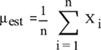
Equation 1
Where n is the number of samples, Xi is the
ith number sample, m is the estimate of the
mean, and Q is the estimate of the
standard deviation. The accuracy of this estimate is directly
proportional to the number of measurements taken.
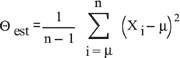
3. Calculate the measurement offset between the sites by calculating
the mean of the Comparison Vector.
The mean is a theoretical value, which is best estimated by taking
an average of the data. (Equation 2)
Equation 2
Where n is the number of samples, Xi is the
ith number sample,mest
and mest is the estimate of the mean. The accuracy of the estimate
is directly proportional to the number of measurements taken.
The measurement variation and measurement
offset calculations describe the past performance between the
pre-compliance setup and the OATS. It is critical that these measurements
are taken with care to accurately characterize the difference
between the two sites. A problem occurs with this when maximized
data is taken at one site and not another. It is important to
compare apples to apples.
Also worth noting is that the 25 samples
required above are just a starting point. The real power of this
process is that it is self-reinforcing. With each unit tested,
more data points can be generated to add to the Comparison Vector.
After enough data is collected, the measurement variation and
measurement offset calculations can be calculated as running quantities,
giving frequency effects more visibility.
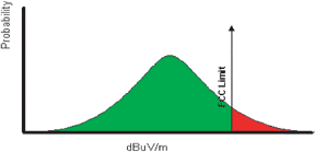
Predicting the Future:
Once the wort is completed, the prediction process is a simple
matter of overlaying a normal distribution curve, defined by the
standard deviation and mean estimated in the wort, onto the measured
data of the unit under test.
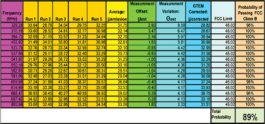
1. Measuring the EUT.
a. Identify the top
10 emissions, and then measure these 10 emissions four more times.
b. Calculate an average reading of each emission.
c. Adjusted the average reading by the Measurement Off set, mest.
m corrected
= m emission + mest
2. Calculate the probability of each individual
emission passing the FCC limit.
The probability of each individual emission passing the regulatory
limit is obtained by integrating the normal distribution up to
the FCC limit using mcorrected as the mean and Qest as the standard
deviation.
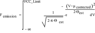
3. Calculate the probability that the EUT will pass the regulatory
limit.
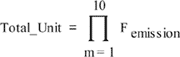
The total probability is calculated by taking the product of
the individual probabilities.
The application of this process is much simpler when put into
a spreadsheet.
This example uses the frequency dependant measurement offset
and measurement variation, which can be done when enough comparison
data is gathered.
The end result of the process is a number 0-100 that “grades”
the unit as to its total likelihood of passing the FCC limit.
In our experience, total probabilities 60 and lower aren’t
worth taking to the OATS. While EUTs with a total probability
above 60 have been consistently passing designs. Our comfort level
has been around 60, but this level will inevitably change for
different companies and different products
Conclusion:
While correlation is important for policing authoritative OATS
sites, it is not necessary for pre-compliance measurements. Using
some basic statistical calculations, on data already gathered
during the standard design cycle, pre-compliance data becomes
a very effective and valuable tool in determining a pass or a
fail. The described approach enables the tester to examine pre-compliance
data and accurately predict if the unit will pass or fail the
upcoming compliance scan regardless of site to site correlation.
Biographies
 Mathew
Aschenberg earned his BSEE degree from Colorado State University,
Fort Collins, Colorado in 1997. He is an Agency Engineer for EchoStar
Technologies Corporation. He has been a member of the IEEE since
1998 and currently serves as Secretary and Vice-Chair Elect for
the Rocky Mountain Chapter of the IEEE EMC Society. Mathew
Aschenberg earned his BSEE degree from Colorado State University,
Fort Collins, Colorado in 1997. He is an Agency Engineer for EchoStar
Technologies Corporation. He has been a member of the IEEE since
1998 and currently serves as Secretary and Vice-Chair Elect for
the Rocky Mountain Chapter of the IEEE EMC Society.
Derrell Gottwald has a Bachelor’s degree in Mechanical
Engineering from the University of Colorado. Since completing
undergraduate studies, he’s taken a number of graduate classes
in applied statistics at CU. Among his professors was Dr. Karen
Kafadar, a well-known statistician who earned her doctorate under
John Tukey at Princeton. Dr. Kafadar’s teaching philosophy,
in part, stresses the importance of collaboration with experts
outside the statistics realm. It is possible for a scientist to
conduct an investigation without statistics, but not so for a
statistician to contribute without understanding the discipline
involved. Derrell thanks Matt and Charles for their time explaining
the nuances of emission testing.
Charles Grasso earned his BSEE degree from Kingston Polytechnic,
London, England in 1977. In 1977, he joined Burroughs Corporation
as a fledgling engineer just as the EMC discipline was beginning
to gather steam. His manager volunteered him as the assigned EMC
Engineer and his life changed from then on. He has worked at StorageTek,
Ansoft Corporation and is currently a Senior Compliance Engineer
at EchoStar Technologies Corporation specializing in circuit/system
design and verification, switching power supply noise and specifications
as they pertain to EMC and Signal Integrity. He is a member of
the IEEE, a member of the dB Society, Vice-Chair and Chair-elect
of the Rocky Mountain Chapter of the IEEE EMC Society.
Errata
Some of you may have noted that there were numerous errors
in Jasper Goedbloed’s paper that appeared in the last
issue of the Newsletter. Further, the figures were printed
with unacceptable resolution. I would like to offer an apology
for both of these. The manuscript supplied by Dr. Goedbloed
was free of any errors and contained figures with fully acceptable
resolution. I take full responsibility for the errors and
the reduction of resolution that appeared in the final version
that appeared the Newsletter. They were introduced in the
editorial process and final checking was not adequate.
We have decided to rectify this situation in two ways. First,
the correct manuscript has been posted on the Web at
https://www.ieee.org/organizations/pubs/newsletters/emcs/summer03/
Second, we want to call to the attention of our readers the
three most significant errors that appeared in the paper.
These are:
1) The equation on the line below Eq. (9), where 'Z-sub-2
=' should be 'Z-squared =',
2) The equation on the line below Eq. (20), where a superscript
hyphen is printed, where a minus sign is needed between the
two cross products, and
3) The correct version of Figure 6 and its caption, where
two dashed line squares are clearly visible has been reprinted
below:
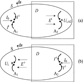 |
| Fig. 6 The states (a) transmission
and (b) reception. The dashed lines indicate parts that
need not necessarily be accessible. |
Robert G. Olsen
Technical Editor
|
Reducing Emissions in the Buck Converter
SMPS
Scott W. Mee
Electronics Engineering, Johnson Controls, Inc. ASG.
Holland, Michigan USA
Email: scott.mee@jci.com
James E. Teune
Electronics Engineering, Johnson Controls, Inc. ASG.
Holland, Michigan USA
Email: james.e.teune@jci.com
Abstract
Switched Mode Power Supply demands
are increasing, as the electronics industry requires more DC-DC
conversion. In the past, linear regulators have been used to regulate
power, but as the difference between supply voltages and desired
output voltage increases, they become very inefficient. The BUCK
power supply is efficient in converting higher voltages to lower
voltages, but unfortunately in the process, both change in current
(dI/dt) and change in voltage (dV/dt) are experienced. These changing
parameters can cause excessive emissions in the RF spectrum, in
conducted and radiated forms. We will examine the modes under
which these emissions are allowed to propagate, and investigate
techniques used to reduce them.
Introduction
One primary contributor to the low frequency emissions is the
switching frequency of the converter, found typically in the 100’s
of kHz range. Energy at the fundamental frequency along with several
of its harmonics can find its way out onto the wire harness and
radiate effectively. These emissions are derived from, among other
things, the sudden changes in current flow (dI/dt) as a result
of the regulator (SMPS IC in Figure 1) turning on and off during
its periodic cycle.
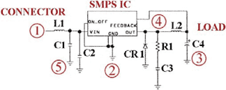
Figure 1. Typical BUCK SMPS Circuit
Diagram.
When the SMPS IC turns ON, the current flows through L1, SMPS
IC, L2, and is delivered to the load (in parallel with C4). When
the SMPS IC turns OFF, the current flowing through the SMPS IC
stops. At this same moment, the energy stored in the inductor
(L2) is released to the load, as the “free-wheeling”
diode (CR1) begins conducting. It is this switching that creates
current flow discontinuities at the input to the power supply.
These current spikes in turn can drive the wire harness, attached
to the product (Position 1 in Figure 1), like a transmitting antenna.
Equation 1 can be used to calculate resonant frequencies (Hertz)
of the cabling; substitute the length of the attached cable (meters)
for l, and the speed of light (3x10⁸ m/s) for C. Using 2, 4, and
20 times the length of the attached cable for l allows other resonant
frequencies to be calculated. If any resonant frequencies of the
cabling correspond with undesired RF frequencies coming from the
Power Supply, the resonance can exaggerate the RF emissions problem.
l = C / f (1)
Equation 1. Wavelength.
Figure 2 shows discontinuities at the input to the power supply
(measuring between VIN of the SMPS IC and ground) while the regulator
is switching. Notice that the discontinuities at VIN correspond
directly to sharp changes in the SMPS IC’s output voltage
(measured between Figure 1 position 4, and ground).
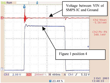
Figure 2. Switching waveforms.
At the output of the regulator (position 4 in Figure 1), dur-ing
switching states, two separate resonant RLC networks can be defined.
These networks produce an under-damped response when “excited”
by a step function (ie. switching!) and allow high frequency ringing
to oscillate for several cycles. Broadband RF emissions commonly
seen anywhere from 40 – 140 MHz are a direct result of this
ringing. The R, L, and C components that make up the networks
are defined by the path that the current flow takes during each
switch state. RLC network #1 is formed when the SMPS IC output
turns OFF. In this state the current flows from ground through
CR1, L2, C4, and the LOAD. Each of these devices has impedance
that is made up of R’s, L’s, and C’s (including
the PCB layout traces and parasitics). When combined, these properties
form the resonant network that gets “excited” by the
step response of the switching (ON - OFF, or OFF-ON). RLC network
#2 is formed when the SMPS IC output turns ON. In this state,
the current flows from the OUT pin of the SMPS IC (Figure 1),
through L2, C4, and the LOAD. Each of these two paths has a unique
frequency response, and is tuned differently. An RC snubber circuit
(R1 & C3) can be added in parallel to the output of the regulator
to create a more “dampened” response in the two unique
RLC networks. If values are chosen correctly, the snubber circuit
will reduce the amplitude and number of cycles of the unwanted
ringing. See waveforms in Figure 3 that illustrate this ringing.
Note the frequency of the ringing is directly related to high
frequency emissions seen during testing (see Figure 4 @ 60MHz).
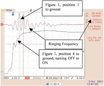
Figure 3. Leading edge, ringing waveforms.
Ringing measured on the output of the regulator (position 4 in
Figure 1) also affects the current flow through the output inductor,
and causes a corresponding change in the magnetic field surrounding
the device. This changing magnetic field can couple onto neighboring
traces or planes allowing the RF energy to proliferate throughout
the board.
Layout Considerations
One of the most important layout considerations for buck converters
is to minimize parasitic capacitance and inductance at the output
of the regulator. Parasitics contribute significantly to the ringing
and other distortion on the output waveform. Do not place a ground
plane on any layer of the board stack-up directly below inductor
L2; this creates the parasitic capacitance that should be avoided.
An option to consider would be to place a power bus (+) beneath
inductor L2 if using a multi-layer board.
Loop Areas
Loop areas need to be controlled and minimized (physical area)
in the layout to reduce overall emissions. A loop formed between
the output pin of the SMPS IC and the ground on the load (connected
across C4) contains large amplitude dI/dt waveforms and must be
controlled to the fullest extent possible. Another loop is formed
between position 1 and position 3 in Figure 1. Finally, a loop
area formed between the input to the supply (position 1) (usually
at the main connector) and the ground to the SMPC IC, contains
small discontinuities (dV/dt and dI/dt). Loop areas are kept small
through proper floor planning and routing of traces. Initially
our output stage (CR1, L2, C4) was not properly designed and the
loop area formed there was approximately 3 in2. Redesigning the
output stage allowed us to reduce the area to 1.5 in2. This change
brought improvements in the amount of cycles and amplitude of
the unwanted ringing on the output (Figure 1 position 4). Although
this was not the only change to the design, reducing this loop
area had a direct correlation to reducing broadband emissions
in the frequency range of 40MHz – 140MHz (Figures 4 &
5).
Feedback Trace
The feedback trace is used by the SMPS IC to sense the status
of its output (connected between C4 and the feedback pin of the
SMPS IC). Therefore, it is critical to route it away from any
noisy circuitry, in particular, the output inductor L2. If using
a multi-layer PCB, the feedback trace of the regulator can be
embedded in a layer below the top layer (further down the board
stack-up) and shielded by ground from the layers above and below.
A ferrite may also be placed in series with this trace to reduce
RF energy that can enter the SMPS IC and can adversely influence
the output waveform.
Component Considerations
Whenever possible, use surface mount devices to minimize lead
inductance. L2 should be a closed core inductor. This type of
component keeps most of the magnetic field confined within the
core during the switching of the regulator. Industry suppliers
have various options to choose from. The best approach is to ask
vendors for samples, and try each type during testing. Choosing
the right device is a key factor in reducing emissions, since
the field surrounding the inductor is constantly changing (i.e.
ringing, switching current) and can couple to neighboring components
and traces, etc.
Snubber Circuit
A snubber circuit can be used in parallel with the output of the
SMPS IC (Figure 1 position 4 to ground) to reduce distortion and
ringing on the output waveform. Typically this circuit is located
between the “free-wheeling diode CR1,” and the output
inductor L2. This circuit works like a high frequency shunt to
allow RF energy to return to ground (i.e. capacitor to ground).
One important factor to consider when choosing to use a snubber
circuit is that you must sacrifice some efficiency in the power
conversion. Some of the power will be dissipated in the snubber
circuit itself. The series resistor is used to limit the amount
of RF current taking this path to ground and the capacitor is
used to “tune” the frequency. The switching waveform
at the location of the snubber circuit is primarily a square wave,
and Fourier theory states that it contains high frequency content
that is dependent upon the rise time of the waveform. Consequently,
without a series resistor in the snubber circuit, there will be
significant power dissipation in the shunt capacitor. The snubber
circuit can be effective at reducing broadband RF emissions typically
seen between 40MHz and 140MHz. Typical values are R = 20 ohms,
and C = .01uf. Also, low parasitic inductance components should
be used to avoid forming resonant tank circuits. Therefore, avoid
using wire-wound resistors, or leaded capacitors.
Diode
The diode (CR1) should be placed on the same side of the PCB where
the other power supply circuitry is placed. This is done in order
to minimize inductance (by avoiding the use of vias) while the
diode is in “conduction” mode and current is flowing
through the diode (CR1) and out to the LOAD (C4). This proved
to be very beneficial for reducing the emissions near 70 MHz.
Diodes that are available in the industry can have various switching
characteristics such as: soft start, ultra slow start and fast
start. These terms refer to how fast or slow the diode switches
from the reverse diode block mode (when the SMPS IC output is
ON), to the forward conducting mode (when the SMPS IC is OFF).
Much of this parameter has to do with the forward voltage required
to “setup” the p-n junction. Tradeoffs must be considered
when selecting the freewheeling diode and the output inductor.
The longer the inductor is in a non-steady state mode, the more
heat it will be required to dissipate.
When selecting diodes from vendors, look for the symbol “Vf”
that indicates the forward voltage required to turn the diode
on. A smaller voltage rating means that the diode will turn on
faster. Each diode has its own characteristic impedance that can
affect the nature of the high frequency emission (40MHz –
140MHz). The process of selecting the right diode can be trial
and error. This is due to the parasitic inductance and capacitance
inherent and unique to each individual layout. If you have test
equipment available, one of the best ways to approach this is
to obtain samples from vendors and place each diode on the PCB
while observing the RF emissions performance.
Front End Filtration
Clean input power is critical for “quiet” SMPS IC operation.
In order to reduce the RF emissions within the low frequency range
(i.e. switching frequency up to several Megahertz), front-end
filtration must be carefully selected. Given that there are two
types of discontinuities seen at the input to the SMPS IC (i.e.
voltage and current), two types of filtering need to be addressed.
Series Inductance
The series inductor (L1) stores energy and releases it as necessary
to reduce current spikes. Caution should be used when selecting
this inductor. First, the device should be properly rated for
steady state current flow. Second, a balance should be considered
between having enough inductance to smooth larger current spikes,
but also keeping a low series DC resistance. Large voltage drops
can occur depending upon current draw, subsequently reducing the
overall voltage available to other circuitry including the SMPS
IC.
Bulk Capacitance
Bulk parallel capacitance is required at the input of the SMPS
IC to remove voltage discontinuities, and should be placed as
closely as possible to the input pins of the SMPS IC. However,
if the bulk capacitor is too large, the charging period will be
long and may cause large current spikes (i.e. higher emissions).
If using Electrolytic capacitors, it is best to choose the lowest
ESR (Equivalent Series Resistance) possible. This ensures that
stored charge is delivered, with the lowest impedance, to the
SMPS IC. In some cases it may be necessary to add a small ceramic
capacitor in parallel with the input between the bulk capacitor
and the SMPS IC. Ceramic capacitors have very low ESR and can
a provide charge at faster rates to reduce unwanted swings in
the voltage.
Common Mode Choke
Common mode chokes are effective input filters. From our experience,
ferrite core CMC’s were effective at reducing emissions in
the ringing frequency range (40 MHz – 140 MHz) but did not
help at the switching frequency (260 kHz). Using an iron core
transformer at the input did the opposite where it adequately
reduced switching frequency noise but did not reduce the ringing
frequency emissions.
Design Methodology
One of the best ways to approach a power supply design is to focus
only on the power supply section initially. Re-move any circuitry
from the PCB that is not related to the power supply. This allows
the designer to implement a layout that is as close to ideal as
possible, given the shape and size of the PCB. An artificial load
can be made to draw the same expected current, as the load will
draw on the board in the power supply’s final application.
The artificial load can be connected during initial testing to
obtain results. We recommend using a conducted emissions test
as a way to benchmark and monitor improvements as the design is
optimized. One primary advantage to this method is that efforts
are focused on the power supply design. Not having the other application
specific circuitry placed on the PCB makes it easier to manipulate
the power supply design. It also requires less time to make changes
and release another prototype revision. After the optimal power
supply design has been determined, the remaining circuitry can
be added. Changing as little of the power supply section as possible
will maintain the improved EMC performance that has been achieved.
Radiated Emissions Comparison
Broadband RF emissions can be seen in Figure 4, in the frequency
range between 40MHz and 140MHz. This broadband “hump”
is attributable to the high frequency ringing on the output of
the SMPS IC. Removing the parasitic capacitance and inductance
found at the output, choosing the appropriate switching diode,
and selecting proper snubber circuit values reduced these emissions.
Figure 5 illustrates improvements in RF emissions gained by optimizing
these design parameters.
Improvements were obtained by the following changes:
-
Decreasing loop areas in all three loops
described in this paper under the heading “Loop Areas.”
-
Used closed core inductor type for L2 instead
of bobbin-wound type.
-
Using low ESR type bulk capacitors for input
(C1, C2) and output filtration (C4).
-
Tuning a snubber circuit to create a more
dampened response at the output of the SMPS IC (position 4 in
Figure 1).
-
Removed ground fill beneath output inductor
L2.
-
Moved diode CR1 to same side of PCB as
other power supply circuitry. Changed diode to On-Semiconductor
“Schottkey” type diode with a forward voltage of
0.51V (i.e. better switching characteristics).
-
Embedded the feedback trace on an inner
layer protected by ground fill, and inserted a series ferrite
placed closely to the feedback pin on the SMPS IC.
-
Make output trace (SMPS IC output to CR1,
L2, and C4) wider to reduce parasitic inductance on the output.
Figure 4. Radiated Emissions (25MHz-200MHz)
– Before.
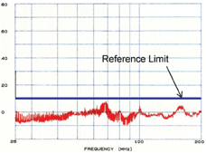
Figure 5. Radiated Emissions (25MHz-200MHz)
– After.
Conducted Emissions Comparison
Figures 6 and 7 illustrate improvements made in the low frequency
range (150kHz – 2MHz) for a Switched Mode Power Supply operating
at 150kHz. In this case the design was using a bulk capacitor
for input filtration, and most of the discontinuities in the voltage
were removed. However, current spikes were still present, and
a series inductor was added to remove current spikes (L1). A value
of 33uH was chosen in order to smooth supply current to the SMPS
IC during switching.
Figure 6. Conducted Emissions (150kHz-2MHz)
– Before.
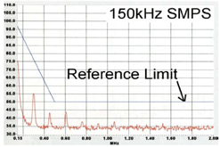
Figure 7. Conducted Emissions (150kHz-2MHz)
– After.
Figures 8 and 9 also illustrate improvements made in the low frequency
range (150kHz – 2MHz) for a Power Supply operating at 70kHz.
The following changes were made to this power supply design to
obtain the improvements:
-
Used closed core inductor type for L2 instead
of bobbin-wound type
-
Reduced loop area from position 1 in Figure
1 to through L1, VIN of SMPS IC, and to the ground of the SMPS
IC. The initial loop area was approximately 3in2; after the
PCB layout changes were made this loop area became less than
1in2.
-
Added a series inductor (L1) to the input
of the power supply (27uH).
-
Routed feedback trace on inner layer shielded
by 1 layer of full ground plane.
-
Added a ceramic capacitor (.01uf) in parallel
with the SMPS IC VIN, between the bulk capacitance (C1) and
the SMPS IC.
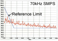
Figure 8. Conducted Emissions (150kHz-2MHz)
– Before.
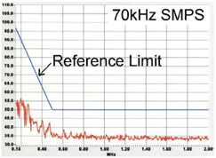
Figure 9. Conducted Emissions (150kHz-2MHz)
- After
Conclusion
Improving the EMC performance of a Switched Mode Power Supply
design requires attention to details in the following key areas:
-
Minimizing loop areas in the layout.
-
Reducing board parasitic inductance and
capacitance due to layout and component placement.
-
Choosing the lowest ESR capacitors available
for input and output filtration.
-
Choosing the correct diode and placing it
on the same side of the board as the other circuitry (minimize
trace inductance).
-
Evaluating the need for a snubber circuit
and tuning it properly.
-
Proper input filtering including proper
series induc-tance, parallel capacitance and/or a common mode
choke.
References
[1] Hnatek Eugene, Johnson Alan, “Designing Electromagnetic
Compatibility Into DC/DC Converters and Switching Regulators,”
IEEE EMC Symposium Paper, (1955-1995)
[2] Jung, Walt, McDonald, John, “Noise Reduction and Filtering
for Switching Power Supplies,” Design Segment, www.sss-mag.com/pdf/ad9.pdf
(2002).
[3] Keith Hardin, Greg McClure, Robert Menke, “Methods for
Identifying Causes of EMI Emissions from Switched Mode Power Applications,”
IEEE EMC Symposium Paper, (2001).
[4] National Semiconductor, “LM2676 SIMPLE SWITCHER‚
High Efficiency 3A Step-Down Voltage Regulator,” National
Semiconductor, www.national.com,
(1998).
[5] National Semiconductor, “LM267X 3A, 5A Evaluation Board,”
Application Note 1135, www.national.com
(1999).
[6] Paul, C.R., “Introduction to Electromagnetic Compatibility,”
John Wiley & Sons, Inc., New York, NY (1992)
[7] Ridley Engineering, “Snubber Circuit Design,” Design
Tips, www.ridleyengineering.com/tips.html
(2001).
[8] SMPS Technology Knowledge Base, “Power Supply Question
and Answers,” Web Based Forum, www.smpstech.com/qa/qa0005.htm
(2000). EMC
Biographies
 Scott
Mee received the BSEE degree from Michigan Technological
University in 1998 with specialties in RF Communications and Discrete
Electronics. Since 1998 he has been working at Johnson Controls
Inc. as a Sr. EMC Engineer. He has over four years of experience
in the automotive EMC industry. His responsibilities include:
EMC product compliance for telematics, multimedia, and other automotive
electronics, product debugging and EMC failure analysis. He has
published and presented technical papers at past IEEE EMC Symposia.
He has also co-authored and published a paper in ITEM magazine
titled: EMC Simulation for the Reduction of Emissions in Telematics
Designs – 2002. His professional interests included EMC software
simulation, product EMC failure analysis, PCB design for EMC,
and EMC test methodology. Scott
Mee received the BSEE degree from Michigan Technological
University in 1998 with specialties in RF Communications and Discrete
Electronics. Since 1998 he has been working at Johnson Controls
Inc. as a Sr. EMC Engineer. He has over four years of experience
in the automotive EMC industry. His responsibilities include:
EMC product compliance for telematics, multimedia, and other automotive
electronics, product debugging and EMC failure analysis. He has
published and presented technical papers at past IEEE EMC Symposia.
He has also co-authored and published a paper in ITEM magazine
titled: EMC Simulation for the Reduction of Emissions in Telematics
Designs – 2002. His professional interests included EMC software
simulation, product EMC failure analysis, PCB design for EMC,
and EMC test methodology.
 Jim
Teune is a Lead Engineer for EMC Test and Design at Johnson
Controls ASG. His responsibilities include directing the EMC design
support activities for product development, technical operations
of the EMC test laboratory (including an Open Area Test Site),
and maintaining Johnson Controls’ AEMCLRP requirements for
automotive laboratory accreditation. He has published and presented
technical papers at past IEEE EMC symposia. He has 15 years experience
working in the area of automotive EMC design techniques and test
methodology. He previously worked with Intel Corporation. He holds
a BSEET from DeVry Institute of Technology and is a NARTE Certified
EMC Engineer. His professional interests include diagnosis of
product EMC issues, and pursuit of methods to recreate field failures
through combined test exposure. Jim
Teune is a Lead Engineer for EMC Test and Design at Johnson
Controls ASG. His responsibilities include directing the EMC design
support activities for product development, technical operations
of the EMC test laboratory (including an Open Area Test Site),
and maintaining Johnson Controls’ AEMCLRP requirements for
automotive laboratory accreditation. He has published and presented
technical papers at past IEEE EMC symposia. He has 15 years experience
working in the area of automotive EMC design techniques and test
methodology. He previously worked with Intel Corporation. He holds
a BSEET from DeVry Institute of Technology and is a NARTE Certified
EMC Engineer. His professional interests include diagnosis of
product EMC issues, and pursuit of methods to recreate field failures
through combined test exposure.
|
 Practical
Papers, Articles and Application Notes
Practical
Papers, Articles and Application Notes