Bob Rothenberg
Associate Editor
This section of the Newsletter is intended to provide EMC practitioners with an outlet for sharing knowledge or perspective gained from experience. To submit an article for consideration, send it via fax, e-mail or real mail to this Associate Editor. See page 3 for addresses and fax number.
The following two articles should be of interest to EMCS members. Herb Mertel describes a verification test program carried out at Oklahoma City Hospital to determine whether the procedures of ANSI C63.18 are simple and practical. Mark Montrose provides some fundamental EMC concepts relating to routing clock traces on printed circuit boards, based on material extracted from two books he has authored: Printed Circuit Board Design Techniques for EMC Compliance (IEEE Press, 1996) and EMC and the Printed Circuit Board — Design, Theory and Layout Made Simple (to be published in 1999).
Reader feedback is welcome, either as a letter (or e-mail) to the Editor or directly to the authors.
by Herbert Mertel
On May 21, 1998, twelve biomedical engineers from various hospitals participated in a workshop to determine whether the methods given in ANSI C63.18 are easily usable. The work was performed at the University Hospital in Oklahoma City. The workshop was preceded by a one day seminar explaining the procedures of C63.18 at the Center for the Study of Wireless Devices, located at the Oklahoma University in Norman, Oklahoma.
The instructors included Sean Boyd, FDA Winchester Engineering and Analytical Center; Don Heirman, Don HEIRMAN Consultants; Herbert Mertel, Mertel Associates; and Jeffrey Silberberg, FDA Center for Radiological Health. The seminar was guided by Dr. Hank Grant and his able staff from the Center for the Study of Wireless Devices.
The testing was performed on the vacant 9th floor of the University Hospital. The testing configuration is shown in Figure 1. An additional item was added: Sean Boyd brought along a Holaday E-Field sensor for up to 2 GHz. The probe was held over the EUT by a participant. This device proved very valuable since it reads out directly in V/m. Consequently, we could measure the field around the EUT whereas C63.18 provides only an estimate of the field strength on the basis of the rated output of the portable transmitter. The field was estimated on the basis of the dipole equation. In general, this was conservative. The measured field strength was always lower than estimated by up to 10 dB!!
Several medical devices were evaluated with various transmitters. The cellular phones were operated at maximum rated power by a maintenance code provided by the Center. The procedure was as follows: at the specified distance (3 m), the transmitter was held at the normal operating height of 1.7 m, polarization was changed from vertical to horizontal, then the transmitter was held at 1 m, and the transmitter operator approached the EUT up to 0.25 m from the EUT while continuously changing the polarization by rotating the transmitter by 90 degrees.
The test was performed with both vertical and horizontal polarization while the transmitter was modulated with normal speech. No susceptibility problems were observed with the 600 mW cellular phones. The operating pressure of a ventilator was changed with an 8 W transmitter and a field of 5 V/m. No patient-connected devices, such as medical telemetry or infusion pumps, were tested. Such devices will be evaluated during the next verification test.
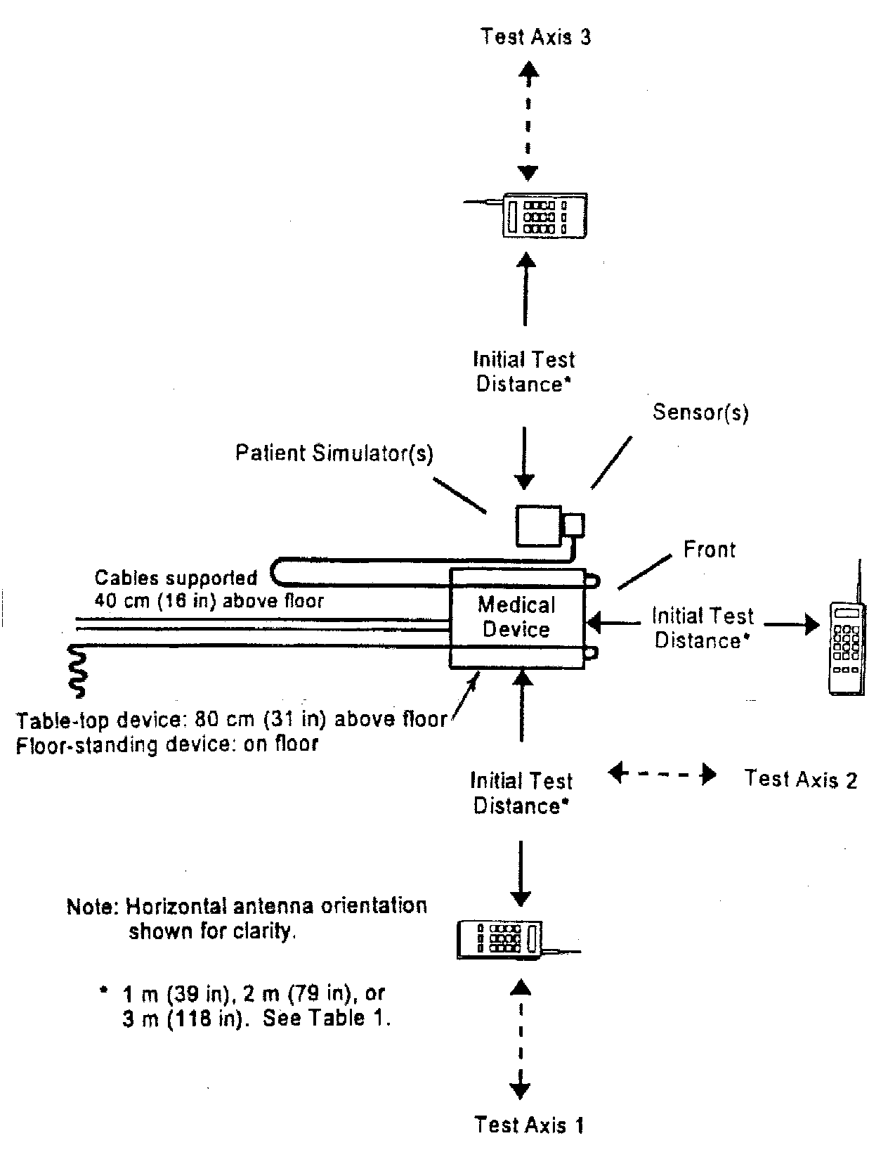
Figure 1
The biomedical engineers participating in the test believe that the writers of C63.18 were overly concerned with the protection of the equipment (i.e. “no damage”). They would like the standard to start the test at the closest distance to the equipment, which can be on top of the equipment. They are confident of being able to fix any damage that might result.
The test also demonstrated that it is imperative to add an E-field indicating device to the test setup, such as a spectrum analyzer with a probe/antenna or an E-field sensor. Most transmitters will have an output that is lower than predicted; therefore, it is important to determine the field strength during the test. For more rapid evaluation of a medical device’s susceptibility, the standard should be changed to an initial test distance of 0.1 meter from the front and rear of the device. At present, no testing at the rear of the device is required.
The C63.18 standard is intended for the use of biomedical engineers who do not have a shielded anechoic chamber available and who want do some quick evaluation of a medical device’s immunity to the small portable transmitters in general use. Therefore, this workshop was a valuable experience for the writers of the standard. The findings will be incorporated in a planned revision of the standard.
The writers of the standard are indebted to the staff of the Center for the Study of Wireless Devices for having arranged the seminar and workshop.
 Herb Mertel is an EMC consultant with Mertel Associates,
P.O. Box 300752, Escondido, CA 92030
(e-mail: hmertel@home.com).
by Mark I. Montrose
This article discusses how to route traces on a printed circuit board (PCB), along with proper component placement. We must be concerned with both the time domain (functionality), and frequency domain (EMI) of any product design. The discussion is applicable to single-sided, double-sided, and multilayer designs.
Oscillators, associated components, and clock traces account for a significant amount of the RF energy generated within a PCB. A clock circuit is defined as the functional area that physically contains the oscillator and/or its buffers, drivers, and associated components, both active and passive. RF energy is observed related to both the rise and fall time of signal transitions, and the fundamental clock frequency of active components. To determine the highest RF spectral distribution of energy typically observed, Equation 1 is used. This equation does not take into account harmonics of the primary frequency.

(Eq. 1)
where fmax = maximum generated RF frequency, and tr = edge rate in ns (use the faster value of either the rise or fall time).
For example, a 2 ns edge rate, typical of common clock drivers and components, can be expected to radiate significant RF energy up to 160 MHz, falling off rapidly above that frequency. The possible significant RF spectrum is 10fmax or 1.6 GHz, which includes the harmonic content of the main frequency component.
Clock and periodic signal traces should always be manually routed before any other action occurs. Following successful manual routing of clocks and sensitive or high-threat traces rich in RF energy, the rest of the PCB can be routed by automatic means.
Locate clock generation components near the center of the PCB, or adjacent to a mechanical ground stitch location (to chassis ground), rather than along the perimeter of the board or near the I/O section. If the clock trace goes off the board to a daughter card, ribbon cable, or interconnect, locate the clock circuit some distance from this interconnect, but not so far away as to make the interconnect trace electrically long. Terminate the clock trace directly at the connector, whether an interconnect is present or not. It is imperative that this be comprised of a single point-to-point connection. Termination of clock lines where a trace crosses a boundary (connector) guarantees signal quality and improves functional performance. Without termination, a clock trace can act as a monopole antenna when no interconnect, or load, is provided. In addition, proper termination of transmission lines helps suppress common-mode induced RF currents from coupling into other areas susceptible to RF corruption. Install oscillators and crystals directly on the PCB rather than using sockets. Sockets add lead length inductance (LdI/dt). Lead length inductance allows ground noise voltage to be created across the transmission line. Ground noise voltage is developed because there may exist a difference in voltage potential between two circuits, caused by inductance in the circuit. Ground noise voltage in turn generates common-mode RF currents, which can radiate, or couple, into susceptible areas.
Locate components that use clocks or periodic signals to achieve the shortest, straight-line path possible (minimal Manhattan length) between two points, with no vias in the trace route, if possible. Ground vias, if required, are discussed later in this article. Each via adds approximately 1-3 nH inductance to the trace route. Inductance in a trace can cause both signal quality concerns (time domain) and potential RF emissions (frequency domain). The total inductance within a trace is added to the sums of all via inductances. The faster the edge rate of the clock signal, the more this design rule becomes mandatory. If a periodic signal, or clock trace, must traverse from one routing plane to another, this transition should occur only at a component lead at 0V, or ground reference, not anywhere else. The reason for making the transition adjacent to a component lead is to allow RF return current to easily make a layer transition jump. Try for a maximum of two vias per route, one at the source, and one at the load, if a stripline configuration is provided.
The old directive to “keep clock lines short” will always be valid. The longer the trace, the greater the probability that RF currents will be produced, and more spectral distribution of RF energy created. Clock traces must be terminated to reduce ringing (enhance signal integrity), and to prevent the creation of avoidable RF currents. Improperly terminated clock signals might also degrade the signal to the point of being non-functional, depending on frequency of operation and logic family provided.
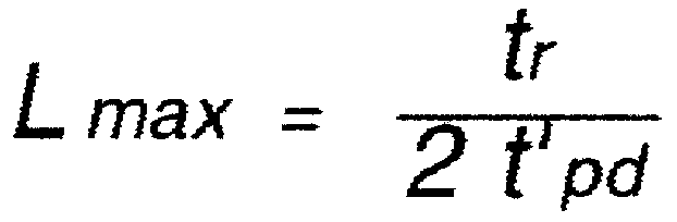
How do we determine if a trace is electrically long? Typical velocity of propagation of a signal in a trace is 60% of the speed of light. From this, calculate the maximum permissible unterminated line length (Eq. 2). This equation is valid when the two-way propagation delay (source-load-source) is greater than, or equal to, the signal rise time. This length is for round trip distance. The one way length, from source to load, is 1/2 the value of Lmax.
(Eq. 2)
where tr = edge rate of the signal transition (ns); t’pd = propagation delay of 1 cm of line (ns); and Lmax = maximum round trip distance of the routed trace (centimeters).
When dealing with transmission lines, a PCB designer needs a general rule-of-thumb during component placement, that allows quick determination of whether a trace route can be considered electrically long. A simple calculation is available with almost absolute accuracy. When determining if a trace is electrically long, think in the time domain, as the propagation speed of the signal is based exclusive on the permittivity, or dielectric constant of the planar material.
To simplify (Eq. 2), there are two basic equations for determining maximum electrical routed length before termination is required. These equations, (Eq. 3 and 4), take into account conversion from units of feet to cm and include the propagation delay, tpd. For FR-4 material, with a dielectric constant of 4.6, the flight time of a signal routed microstrip is tpd = 1.72 ns/ft and for stripline tpd = 2.2 ns/ft. If the routed trace length is greater than Lmax, both signal functionality and EMI concerns exist.
Lmax = 9 tr (for microstrip topology - in cm.) (Eq. 3)
Lmax = 3.5 tr (for microstrip topology - in inches)
Lmax = 7 tr (for stripline topology - in cm.) (Eq. 4)
Lmax = 2.75 tr (for microstrip topology - in inches)
For example, if a signal edge is 2 ns, the maximum unterminated trace length for routed
microstrip is Lmax = 9 tr = 18 cm
(7"). When this same clock trace is routed stripline, the maximum unterminated trace
length of this 2 ns signal edge is now: Lmax = 7tr
= 14 cm (5.5").
For materials with a dielectric constant other than 4.6, the propagation delay of a signal
within a trace will differ. To use a different dielectric constant value, (Eq. 5) is
presented.

(Eq. 5)
where: a = 30.5 (for cm) or 12 (for inches); and x = 0.5 (converts transmission line to one way path). The equations for propagation delay of a signal are
tpd = ![]()
for microstrip, and
tpd = ![]()
for stripline, with er the dielectric constant of the material at the frequency of operation. For example, if er = 4.1, Lmax = 8.9 cm (3.5 in.) for microstrip, and 6.9 cm (2.7 in.) for stripline.
If a trace is longer than Lmax, termination is required, as signal integrity concerns, reflections and ringing may occur. Ringing generated by an impedance mismatch in an electrically long trace may also make the circuit non-functional, and could create common-mode RF currents within the trace. (The signal of interest is usually differential mode.) Even with optimal termination, a finite amount of RF current will exist in the trace due to the potential difference between the source and load circuit.
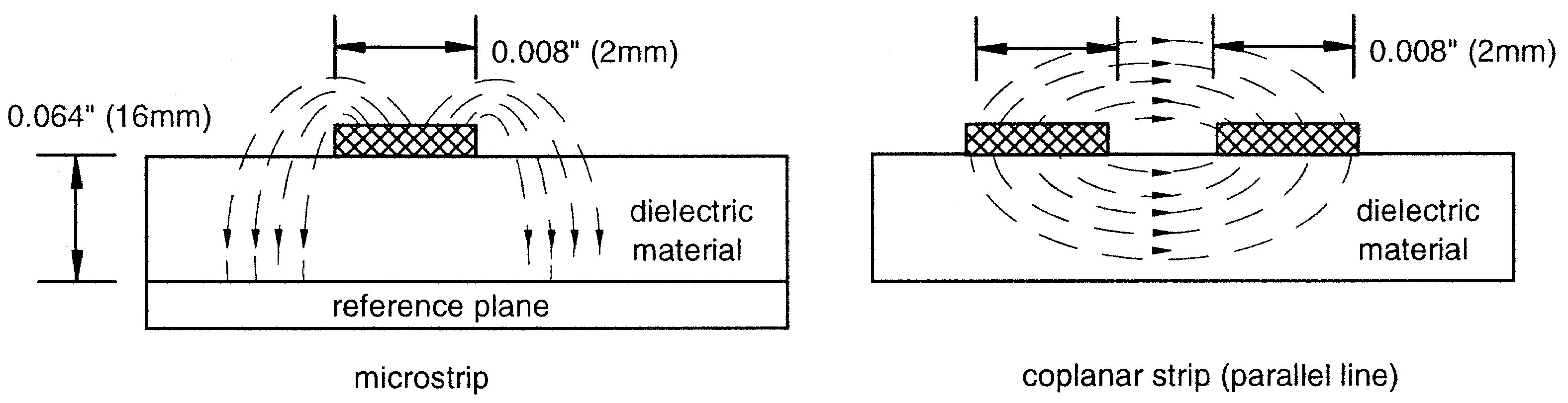
Figure 1. Field distributionh for microstrip and coplanar strips
For every signal, a time domain reflection occurs. It takes a finite time for a signal to travel from source-to-load, and then return from load-to-source. An electrically long trace is a trace that allows the one way (source-to-load) propagation delay to exceed 1/2 the clock cycle. If a second clock signal (edge transition) occurs before the reflection of the original signal returns to the source, signal integrity problems occur. Depending on the phasing of the reflection, overshoot or undershoot may develop, which affects signal integrity. Signal degradation is a concern if the edge time of the signal constitutes a significant percentage of the propagation time between the device load intervals. Proper termination prevents ringing and reflections from occurring, thus enhancing signal functionality.
When designing any PCB, one must take into consideration several major concerns. These concerns relate to optimal signal integrity along with EMC compliance.
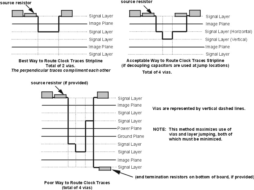
Figure 2. Routing Layers for Clock Signals
For single- and double-sided PCBs, it is virtually impossible to create an optimal transmission line. The impedance of a typical trace on a single- or double-sided PCB is 110 to 135 ohms. When used in a 50 ohm circuit, this impedance mismatch may cause the system to become non-functional, especially if the system clock is greater than 10 MHz, or clock edges are faster than 5 ns. In addition, an optimal RF return path may not be present in a single-sided design, whereas in a double-sided assembly, the distance between the trace and the RF return path is excessively large, typically 0.16 cm (0.062").
RF flux present on a trace is generally observed at a distance that is equal to the width of the trace. RF flux from a 0.008" trace will couple easily to an image plane that is 0.008" away, instead of a plane 0.062" away. Because of the current density distribution of RF flux, related to a RF return path, use of single- or double-sided PCBs is not recommended for any high-speed design. Figure 1 illustrates RF field distribution for microstrip traces. For a double-sided PCB, RF flux must travel through a dielectric material to find the RF return path. If a trace at 0V potential is routed adjacent to the clock trace on a single-side design (coplanar configuration), the trace becomes the RF return path. There is no simple technique for routing single- and double-sided PCBs that are EMI compliant due to: lack of an optimal RF return path, high trace impedance, and lack of a proper transmission line. Although use of a simple stackup assignment is cost effective, additional cost will probably be required through use of shielding or containment of internally created RF energy. It is generally cheaper to add a power and ground plane to a PCB, than to rely on secondary shielding methods.
For multilayer designs, clocks and periodic signals must be routed adjacent to a solid plane, preferably at ground or 0V potential. A plane must not be floating or isolated. This is true for both routing layers, “x” axis and “y” axis (also identified as the horizontal or vertical routing planes). When selecting routing layers, the designer must be concerned with which layers to use for trace routing, jumping between designated layers, and maintaining constant trace impedance.
Figure 2 shows an example of how to optimally route clock traces on different layers, assuming a multilayer stackup. The following design guidelines are suggested:
1. A solid (image) plane is located adjacent to the routing plane, or signal trace. Minimize routed trace length while maintaining constant trace impedance of the transmission line. If series termination is provided, connect the resistor directly to the output pin of the component. After the resistor, place a via to the internal stripline layer(s). The use of ground planes is preferred over use of voltage planes for the following reason: Voltage planes generally contain switching noise injected by components into the power distribution system. The voltage plane may disrupt the RF return path or cause common-mode coupling of switching noise into the RF return path.
2. Do not route clock or sensitive traces on the outer layers of a multilayer board, if a six or more layer stackup is provided. The outer layers of the PCB should be reserved for large signal busses and I/O circuitry. Functionality and signal quality of these traces could be corrupted by routing high-threat signals microstrip. When routing traces between layers, there will be a change in the characteristic impedance of the trace, as the trace relates to a reference plane (impedance control), thus affecting performance and possibly causing signal degradation.
If the design maintains constant trace impedance, provides for an optimal RF return path, and minimizes or eliminates use of vias (reduce inductance), the trace will not radiate any more than a coax.
When routing clocks or high-threat signals, it is common practice to via the trace between routing planes (e.g., x-axis) and then via this same trace to another plane (e.g., y-axis) from source to load. This is shown in the poor routing method of Figure 2. It is generally assumed that if each and every trace is routed adjacent to an image plane, or RF return path, there will exist tight RF coupling (flux cancellation) of common-mode RF currents along the entire route. In reality, this assumption is incorrect.
When a jump is made from a horizontal to a vertical routing layer, the RF return current cannot make this jump. This is because a discontinuity occurs in the trace route by the via. The RF return current must now find an alternate, low inductance (impedance) path to complete its return. A suitable alternate path usually does not exist when jumping a trace between layers. To minimize creation of EMI and crosstalk, due to layer jumping, the following design techniques have been found to be effective:
A ground via is a via that is placed directly adjacent to each signal route via at one trace width distance away. Ground vias can only by used when there are multiple ground planes in the PCB. This via must connect all ground planes together. Ground vias guarantee that a constant RF return path is adjacent to a signal route, thus providing a mechanism for optimal flux cancellation. The ground pin of a component makes an excellent ground via.
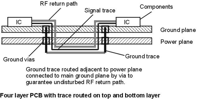
Figure 3. Using a ground trace on a four-layer stackup
For a four-layer PCB, with one voltage plane and one ground plane, how is a constant RF return path provided when a ground via cannot be used? To maintain a constant return path for RF currents, the 0V reference plane must be allowed to act as the primary return path. When the trace must route against the power plane, use of a ground trace is required, with vias at both ends of the ground trace routed parallel, and adjacent, to the signal trace tied to the 0V reference plane. Using this configuration, a constant RF return path can now be maintained, as detailed in Figure 3.
The important concept for routing traces with periodic signals is to provide a properly terminated, impedance controlled signal route adjacent to an RF return image plane. This image plane provides for flux cancellation of RF common-mode currents, and allows the trace to function as a coaxial transmission line. Ground vias allow the RF return path to be undisturbed along the entire trace route. If multiple ground planes are not provided, a ground trace must be used on the routing plane adjacent to the signal trace to assure a constant, undisturbed RF return path.
 Mark Montrose can be contacted
via telephone at (408) 247-5715,
or via e-mail at mmontros@ix.netcom.com.