A practical approach to the design of broadband absorbers starts with a lower frequency ferrite tile material of commercial use for the 30 MHz - 1 GHz frequency range, and then considers a second layer, to be determined, so as to improve the absorber performance and especially to extend the higher frequency limit.
In a two-layer absorber, it is convenient to consider a given first layer (against ground plane), as for example a commercially available 30 MHz - 1 GHz ferrite tile, of given material and thickness. This will determine the surface impedance, Z1sc, on top of this first layer. Any discrepancies with free space impedance will now have to be compensated for with a second (flat) layer, with the purpose of achieving the high frequency performance increase. In other words, the surface impedance, on top of this second layer, is to be “driven” to the free space impedance, i.e.:
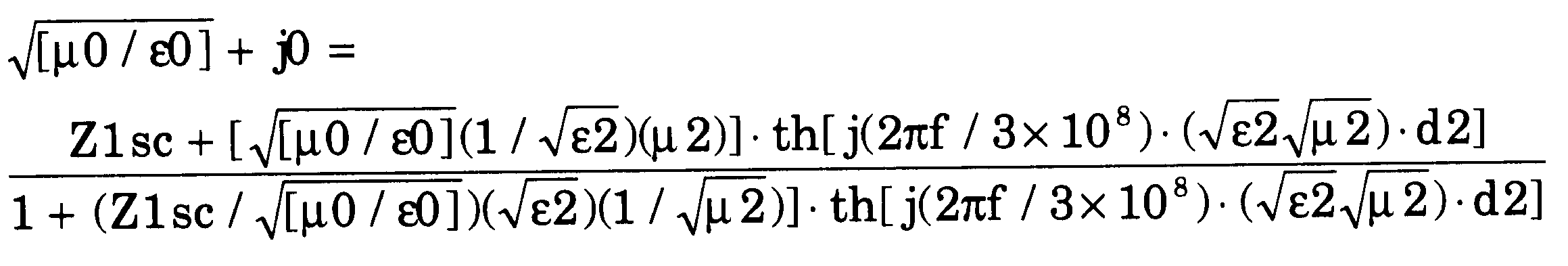
where m0 and e0 are the permeability and permittivity of free space, f = frequency, and e*2 = eó2 – jeóó2 represents the permittivity of its second layer, m*2 = mó2 – jmóó2 its permeability, and d2 is the thickness. Z1sc represents the first layer surface impedance.
The analysis of this equation demonstrates the need for layered materials, of wave impedances higher than the impedance of air, in a frequency area where m* values are small. The analysis is simplified by the need to consider only low e* values, which for practical reasons can be non- dispersive (i.e., eóó2 = 0). One can then calculate “ideal m*2 (w) spectra” for a given e*2 with the thickness d2 as parameter. Figure 1 shows such a spectrum with a first layer 42 ferrite (representative of any commercially available 30 MHz - 1 GHz tile), of thickness 6.3 mm, as well as related wave impedance spectra which must be “hi-Z” materials, with wave impedances higher than one, up to the highest frequencies involved.
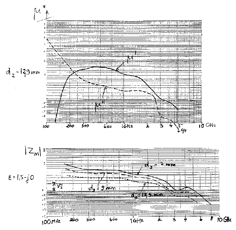
Figure 1.
The feasibility of the “cloning” of such ideal m*2 spectra involves now known and possibly new magnetic material science. To the physicist, a priori, the cloning is possible between some 600 MHz (as long as mó2 becomes dispersive), and some 8 GHz (where móó2 is positive).
A typical example of the cloning procedure for the second layer is shown in Figure 2 (which must be superimposed on Figure 1 to check the correlation). Figure 2 is relative to a low density ferrite grain assembly (with eóó2 ~ 1), using two kinds of ferrite:
Ferrite a of a Ni-Zn stoechiometry composition
Ferrite b of a Mn-Zn sub-stoechiometry composition (so as to have high resistivity)
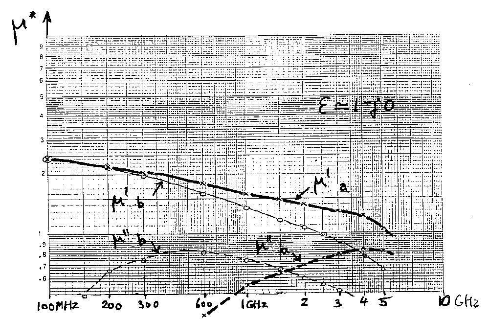
Figure 2.
If the mó2 spectra are comparable, the móó2 spectra are quite different. The figure shows clearly that the best móó2 cloning is performed with some mix of both ferrites. Nevertheless, the mó2 values are “disconnected” from móó2 values; indeed, such low volume concentration of the grain assemblies show preponderant demagnetization effects, and móó2 does not reach mó2, as normally expected.
A solution consists of using oriented grain structures, oriented oblate particles or even radically uniaxially anisotropic structures, such as ferrite posts or ferrite wafers, oriented in the axis of propagation.
Figure 3 shows the m*2 spectra super- posed on the ideal m*2 spectra, for the Ni-Zn ferrite above, where particles are arranged in a bulk ferrite array oriented by a DC magnetic field, so as to form the “Hi-Z” outer layer. The corresponding implementation, with a thickness d2 of 12.9 mm, which corresponds to a good broadband correlation, shows the reflectivity spectra of Figure 4, with an excellent reflectivity (> 15 dB) from 25 MHz to over 5 GHz.
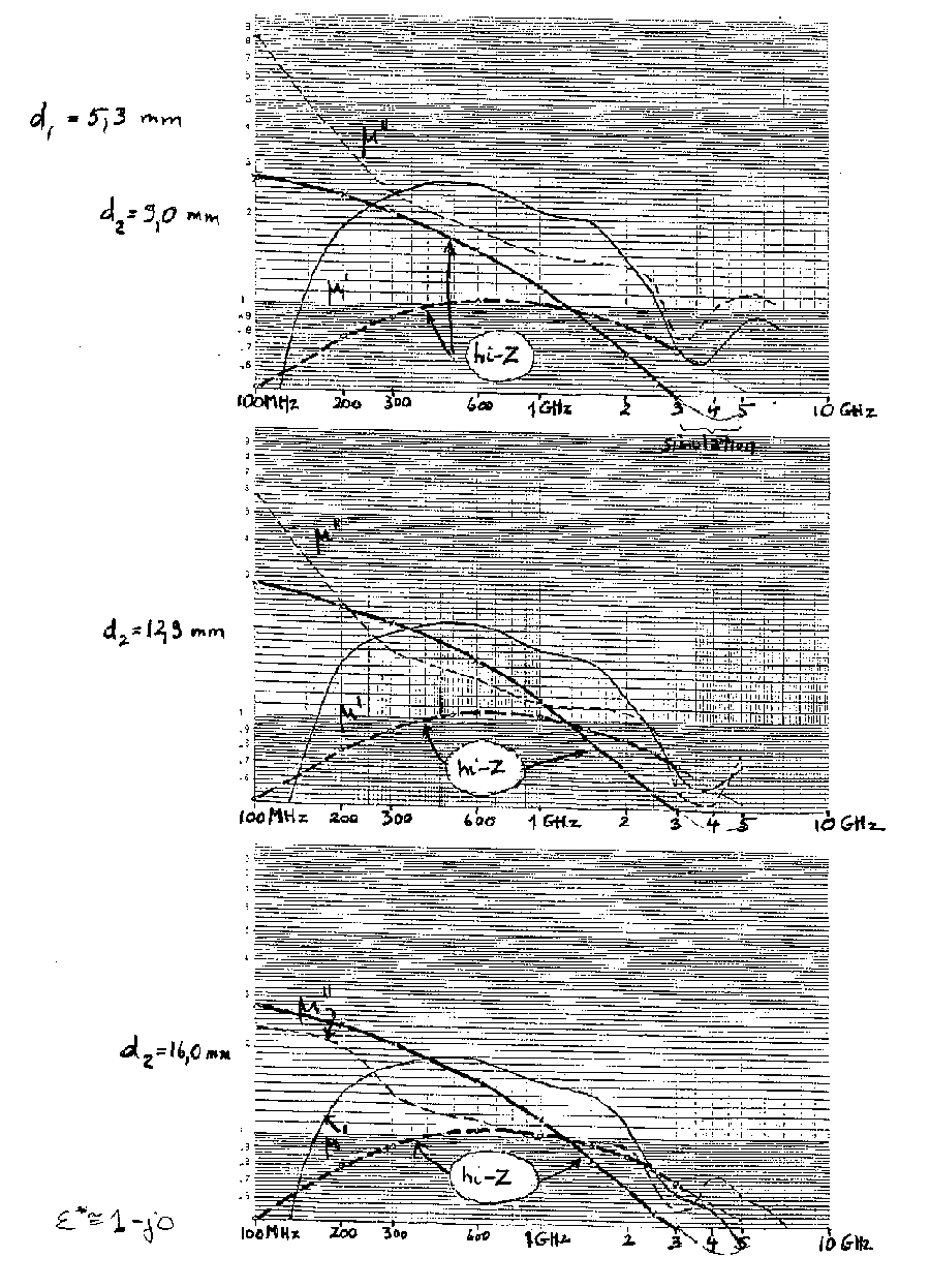
Figure 3.
The optimization of such a cloning can now use more or less sophisticated techniques, where nevertheless we have to consider that theoretical formalization of such new mixes/shapes/structures of magnetic layers are not currently available. We shall present the theoretical modelization in a future publication.

Figure 4.
In a first approach to such an optimization, we have completed the Figure 1 “ideal m*2 spectra” (achieving infinite reflectivity), with the limits of the deviations of:
mó2 considering móó2 as having the ideal values, and
móó2 considering mó2 as having the ideal values.
so as to achieve 20 dB reflectivities (Figure 5).
More complicated “double optimizations” are now under study. In a first application of this technique, we have achieved an over 25 dB reflectivity, using a second layer of a uniaxially partially anisotropic porous ferrite, of thickness 9 mm.
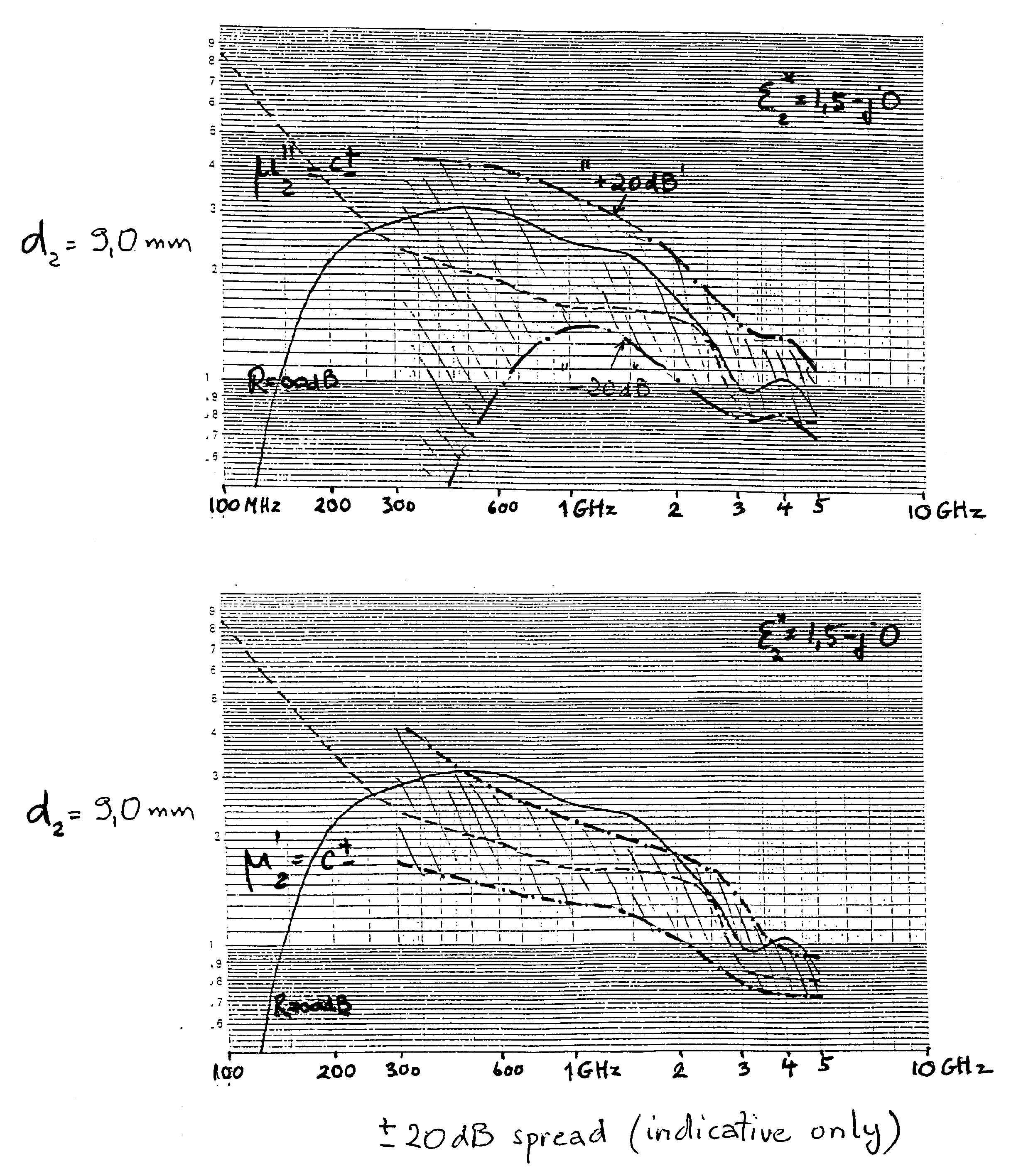
Figure 5.
We emphasize the need for an understanding of more complex non-isotropic magnetic
structures, including intrinsic anisotropic, shape and structure anistropic, and
bi-anisotropic new materials (Figure 6). Details are given in French patent application #
98/114.70, of September 16, 1998, and related foreign patent applications.
The development of the “inverse-approach” and the knowledge of the spectra of
such new materials will be an important incentive for new approaches to broadband
electromagnetic wave absorbers.
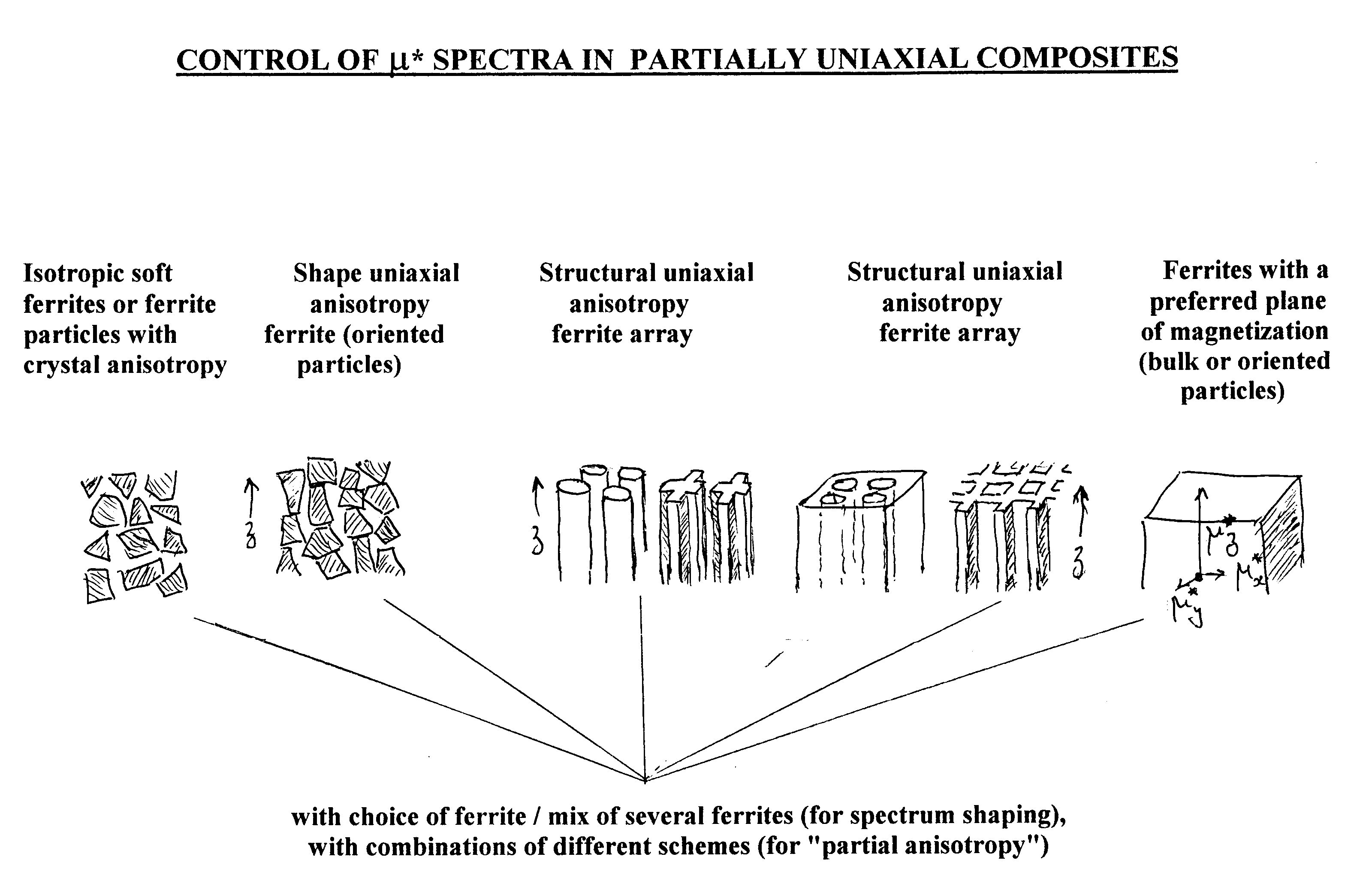
Figure 6.
 |
 |
 |
| Dr. Mayer | Dr. Berthon | Dr. Perini |
Dr. Ferdy Mayer is Chairman of the IEEE EMC Society’s International Committee and an Honorary Life Fellow of the IEEE. He can be reached at FerdyMayerLEADFrance@compuserve.com. Dr. Berthon is Chairman of Club 25 of SEE France. Dr. Perini was a Professor at Syracuse (NY) University, until his retirement in 1991.