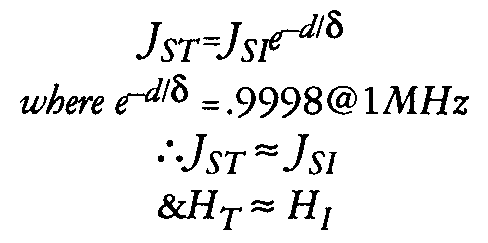
The industry uses "shielding effectiveness" as a "figure of merit" for gauging the attenuation of an electromagnetic field through shielding barrier material. The concept of shielding effectiveness is based on wave theory, where the math associated with the theory is abstract and does not lend itself to understanding the physics associated with the penetration of the field through the barrier material.
By using circuit theory to calculate the attenuation associated with the penetration of an electromagnetic field into and through shielding barrier material, the physics associated with the penetration can be realized. It can also be used to approximate the value of the E and H fields at any given distance from the barrier as a function of the H field impinged on the incident side of the barrier.
A demonstration was presented at the 1999 IEEE International symposium on EMC in Seattle. An explanation of the presentation and results is contained herein.
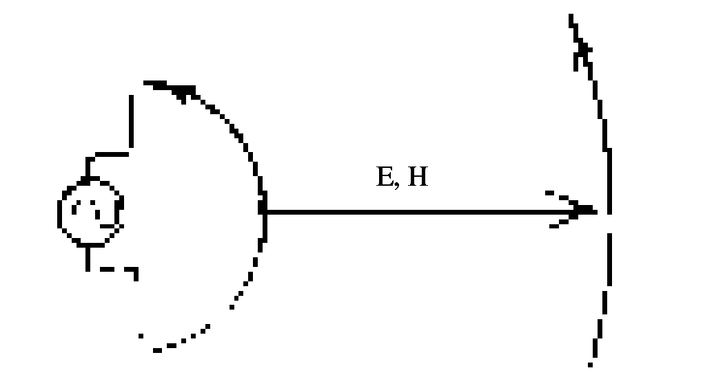
A radiated electromagnetic field is generated by the action of driving a current through a wire. The EMC community typically uses a dipole (electric and magnetic) antenna to generate the field of interest.
Figure 1 illustrates a typical electric dipole antenna, which is being driven by an ac voltage source.
|
Figure 1. Generation of EM Field |
What is illustrated is the generation of a radiated force field created by a differential of voltage potential from the energy source. This force field consists of an electric "E" field, which is a function of the difference in voltage between the ends of the antenna, and current, which is a function of the capacitive reactance between the ends of the antenna. There is also a magnetic "H" field, which is at right angles to the force field. The current, which is parallel to the E field, is measured in units of amperes/meter and is equivalent to the value of the H field.
The field moves away from the antenna, with the power in the field decreasing as the square of the distance. Figure 2 illustrates the field (or wave) impinging on a shielding barrier.
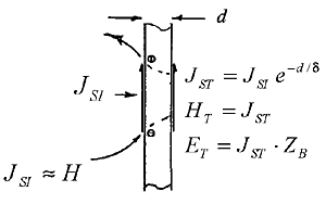 |
Figure 2. EM Field Penetrating Barrier |
Current is induced into the barrier material. Its value is approximately equal to the value of the H field incident on the barrier. This current is reduced in value by a force called skin effect as the field penetrates the material. The value of the E and H fields as the wave leaves the barrier is equal to the value of the fields on the surface and is as illustrated in Figure 3. Since the current (H field) lags the voltage (E field) by 45°, the power of the transmitted field is as follows:
The power of the field decreases as the square of the distance from the original source of energy (i.e., dipole antenna). The value of the power and the value of the E and H fields at a distance R2 can be approximated using the equations of Figure 3.
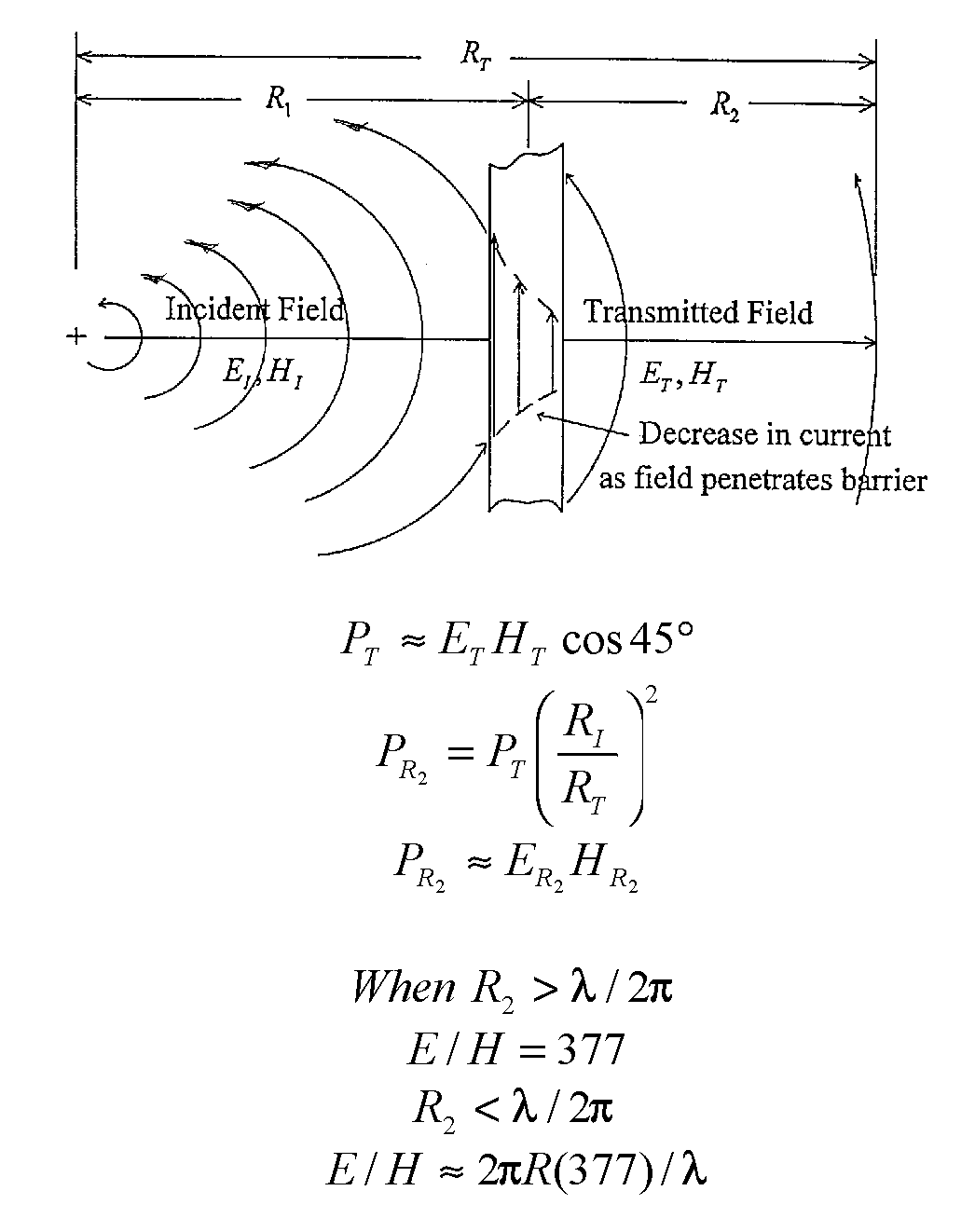 |
Figure 3. |
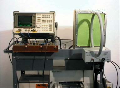
In the demonstration, the H field generated by an electric dipole antenna situated in a shielded box (with the face open), as illustrated in Figure 4 is measured over the frequency range of 100 kHz to 1 MHz. A shield consisting of aluminized mylar measuring 1.4 ohms is then attached to the face of the box. The strength of the E and H field with the shield over the opening of the box, as illustrated in Figures 5 and 6, is then measured. The measured values are compared with the predicted values for the H field without the shield in place. The shielding effectiveness for the E field is also measured.
 |
 |
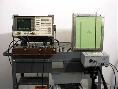 |
Figure 4. Configuration for Testing H Field with Cover Off |
Figure 5. Test Configuration for Measuring H Field with Shield Material Over Face of Box |
Figure 6. Test Configuration for Measuring E Field with Shield Material Over Face of Box |
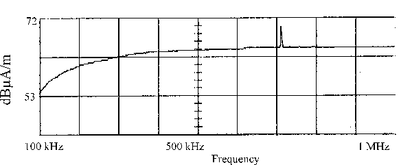
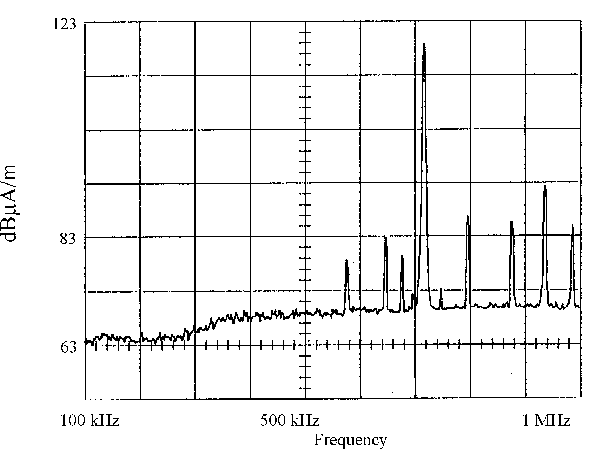
Figures 7, 8, and 9 illustrate the measured field strength before and after the placement of the shield on the face of the box. Figure 10 illustrates the measured field strength of the E field prior to and after the placement of the shield material on the face of the box. The shielding effectiveness to the E field is the difference between the two readings.
 |
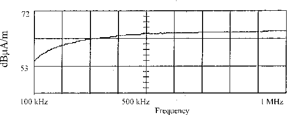 |
Figure 7. H Field Test Data with Face of Shielded Box Open |
Figure 8. H Field Test Data with Shield Attached to Face of Box |
 |
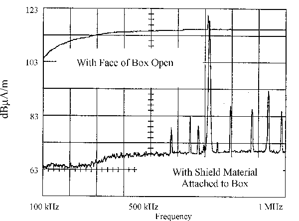 |
Figure 9. E Field Test Data with Shield Attached to Face of Box |
Figure 10. E Field Test Data |
1. The H field before and after the placement of the shield material on the face of the box is the same (as illustrated in Figures 7 and 8). This is as one would predict based upon the conditions described in Figure 2, i.e.,
|
2. The measured transmitted E field over the frequency range of interest is as illustrated in Figure 9. The predicted field strength is equal to measured H field (dBµA/m), the attenuation due to skin effect (dB) plus 20 log 2.4 (dB). The measured and predicted electric (E) field strengths in dBµV/m are as follows:
| Frequency | 66 kHz | 500 kHz | 1 MHz |
| Measured | 63 dB | 69 dB | 69 dB |
| Predicted | 66 dB | 72 dB | 73 dB |
3. The measured E-field shielding effectiveness is illustrated in Figure 10, and is as follows:
| Frequency | 100 kHz | 500 kHz | 1 MHz |
| Shielding Effectiveness |
42 dB | 46 dB | 46 dB |
To obtain the results illustrated in the demonstration, the following calculations had to be performed: (1) the thickness of the aluminum shield material; (2) the impedance of the aluminum shield material over the frequency range of 100 kHz to 1 MHz; (3) the skin depth of aluminum shield material from 100 kHz to 1 MHz; and (4) the normalized values of the recorded E and H fields as a function of the antenna correction factors.
The dc resistance of the aluminum foil was measured to be 1.4 ohms per square. The definition for the dc resistance of a material is
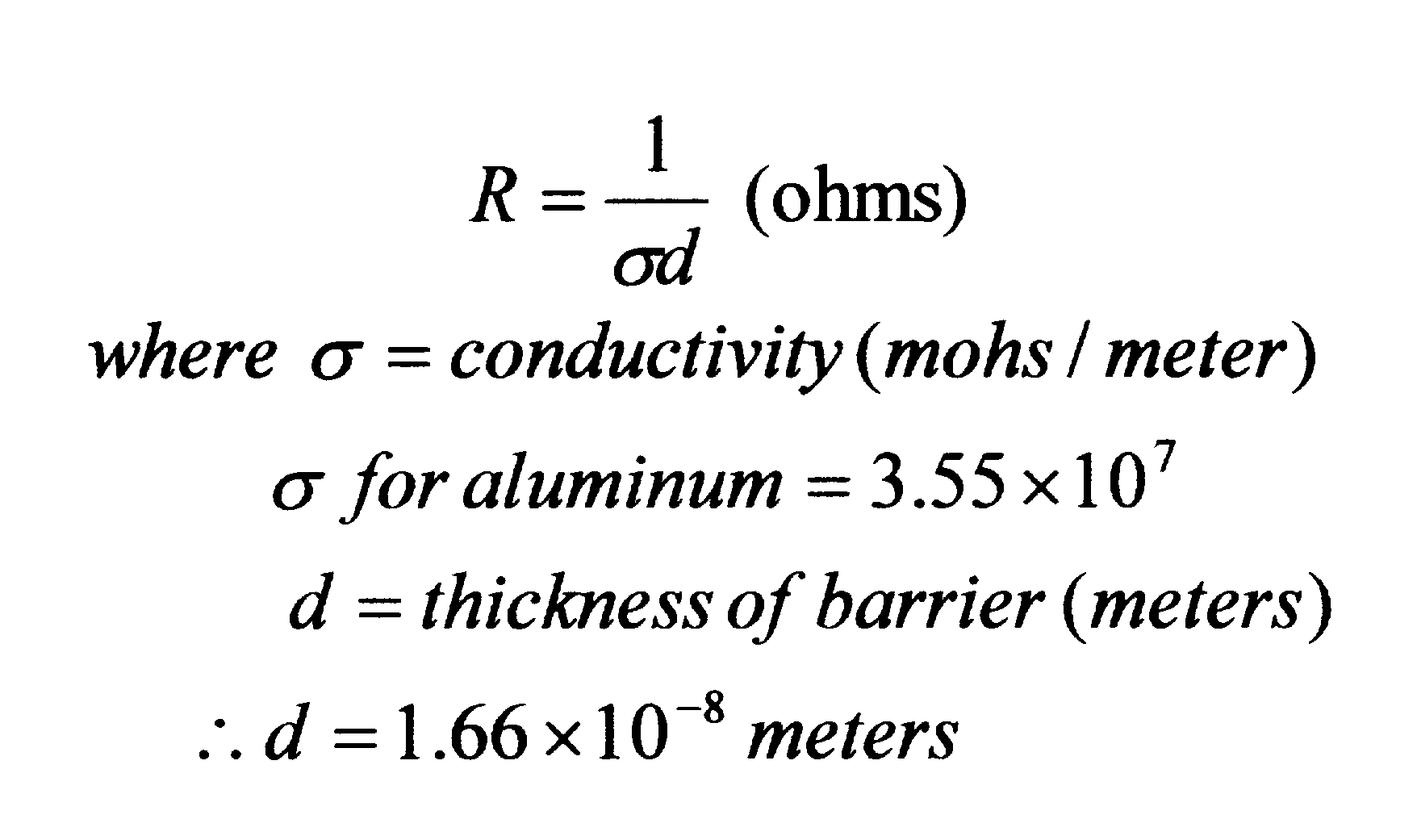 |
The skin depth
is equal to the following:
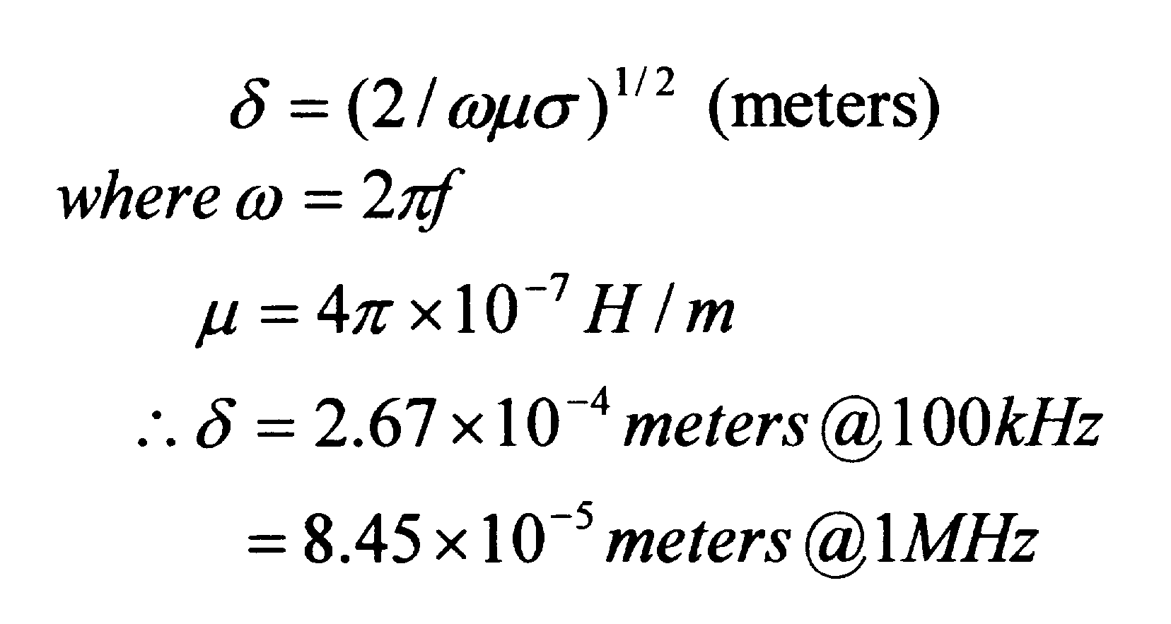 |
The impedance of a metallic barrier material is:
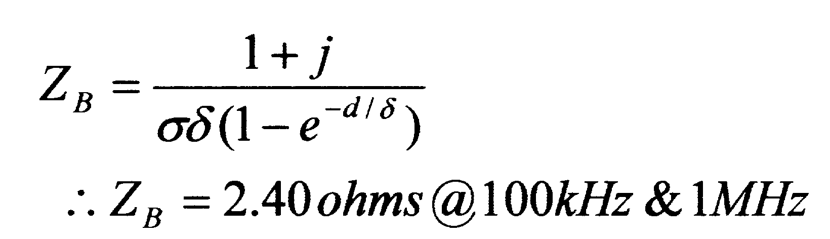 |
The correction factors to be added to the recorded trace from the spectrum analyzer in dB µV are as follows:
The reading at the top line of the spectrum analyzer plot was 107 dB µ V. Therefore the values of the top line of the plots presented herein are:
 |
George Kunkel received his Bachelor of Science and Master of Science degrees in engineering from the University of California at Los Angeles (UCLA). After graduation he taught courses on applied electromagnetic theory in the UCLA extension department. He is presently a member of the Deans Council, College of Engineering at UCLA, and president of Spira Manufacturing Corporation.
Mr Kunkel has nearly 50 years experience as a design engineer, primarily in electromagnetic effects (i.e., EMI/EMC, TEMPEST, EMP, lightning and RADHAZ). He is a senior member of the IEEE and was chairman of the Technical Committee on Interface Control for the EMC Society from 1969 through 1987. He has published numerous papers on grounding, bonding, shielding and filtering.
George can be reached at (818) 764-8222 or via e-mail at george@spira-emi.com. EMC