In this issue you will find one practical paper that should
interest members of the EMC community. It is entitled
“Electromagnetic Emissions of Integrated Circuits
and PCBs” by Jerzy F. Kolodziejski and Juliusz Szczesny.
In this paper, the authors discuss the sources of electromagnetic
emissions from integrated circuits and PCBs that appear
as conducted and radiated electromagnetic disturbances
over a broad frequency range. This paper was originally
presented as, “Use of power supply currents for electromagnetic
compatibility investigation of digital integrated circuits”
at the XVI International Wroclaw Symposium and Exhibition
on Electromagnetic Compatibility, June 25-28, 2002 and
has been revised and reproduced here by permission. In
addition to this paper, I wholeheartedly recommend that
you read the paper by Keen, Tesche and Butler on the Clemson
EMC course that appears in the Education Section of this
Newsletter. Had it not appeared there, I would have been
pleased to have it printed in this section. Our profession
would benefit tremendously if all of our EMC courses were
of as high quality as this one.
The purpose of this section is to disseminate practical
information to the EMC community. In some cases the material
is entirely original. In others, the material is not new
but has been made either more understandable or accessible
to the community. In others, the material has been previously
presented at a conference but has been deemed especially
worthy of wider dissemination. Readers wishing to share
such information with colleagues in the EMC community
are encouraged to submit papers or application notes for
this section of the Newsletter. See page 3 for my e-mail,
FAX and real mail address. While all material will be
reviewed prior to acceptance, the criteria are different
from those of Transactions papers. Specifically, while
it is not necessary that the paper be archival, it is
necessary that the paper be useful and of interest to
readers of the Newsletter.
Comments from readers concerning these papers are welcome,
either as a letter (or e-mail) to the Associate Editor
or directly to the authors.
|
Electromagnetic Emissions of Integrated Circuits and PCBs
Jerzy F. Kolodziejski, Juliusz Szczesny
Institute of Electron Technology
Al. Lotników 32/46 02-668 Warszawa, Poland
Tel. (48-22) 5487796, fax (48-22) 8470631
E-mail: jekolo@ite.waw.pl
There are at least a few reasons for the growing
interest of electronic components manufacturers and users in the
electromagnetic compatibility (EMC) of these components. Among
them of great importance are: increase of packaging density of
electronic circuits, lowering the levels of useful signals in
respect to the background fluctuations (noise) level, and the
rise of speed and functional complexity – above all in integrated
circuits (ICs) and particularly digital ICs.
Talking about the EMC properties, one should take into account
the two sides of the problem – electromagnetic emission (EME)
and electromagnetic immunity (or susceptibility) of the considered
objects. The first question will be discussed shortly in this
paper. Illustrative examples will relate to digital integrated
circuits and to the printed circuit boards (PCBs) with ICs. Both
conducted and radiated emissions will be considered.
Electromagnetic Emission of Printed Circuit
Boards
Electric circuits on PCBs, which can produce EME, are composed
of ICs, cooperating active and passive components, connecting
traces, power, control and signal lines as well as I/O ports and
attached cables. The EME is caused by functional activity of ICs
and other active components and by the flow of time varying electric
currents.
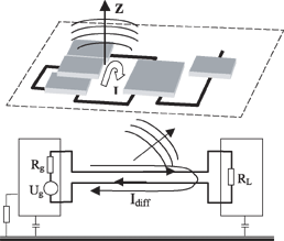 |
| Fig. 1. Differential mode electromagnetic
disturbances generated by current loops inside the PCB circuits |
Electromagnetic disturbances generated by current
loops inside the circuits on PCBs, Fig. 1, have the characteristics
of differential-mode signals in the systems with forward and return
conductors. The current loop can be considered as a small frame
antenna that creates in its close vicinity an electromagnetic
field with a dominant magnetic component. The dimensions of the
small loop antenna should be smaller than a quarter wavelength
of the radiated signal (e.g. < 100 cm at 75 MHz and <10
cm at 750 MHz). If the loop area is around several square centimetres
and the loop current is a few tens of milliamps, then at the frequencies
higher than 30 MHz, the EME levels could exceed the limits in
European Standard EN 55022 for class B equipment (for residential
area). In this situation, it would be strongly recommended to
lower the frequency of useful signals, reduce current values and
limit the area of current loops. If these means could be impractical,
e.g. for the reasons of other requirements, the application of
shielding should be considered. Common-mode disturbances are caused
by unwanted voltage drops, appearing in the systems with cables
and conductors used as the forward path of the signals, and with
the reference (ground) plane, which serves as the return path.
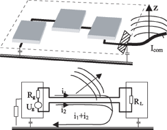 |
| Fig. 2 Common mode disturbances generated
in the systems with cables and conductors, which are the forward
path of the signals, the ground becomes the returning path |
The voltage drops may be related to the voltage
difference between the reference plane (local ground) and module
or equipment ground, Fig. 2. The attached cables and conductors,
working as the rod antennas, mostly radiate high frequency common-mode
disturbances. It is usually assumed that the common-mode impedance
of cables or longer traces on the PCB is approximately 150 W.
Frequencies of emitting disturbances may depend on the cable resonance,
appearing above few tens of MHz. It is always difficult to foresee
the paths of common-mode currents within the circuit, since some
weakly controlled parasitic elements, mainly capacitances, often
participate in the current flow to the ground. Significantly lower
values of common-mode currents, in comparison to differential-mode
currents, can produce EME that exceeds the limits given in EN
55022.
Integrated Circuits as the Source of Electromagnetic
Emissions
Complex and fast ICs such as microprocessors, microcontrollers,
digital signal processors and various ASICs, often have large
transients in the supply currents. It is then justified to treat
the question of EME of the integrated circuits in the same manner
as in the case of PCBs. Emission levels are higher for larger
currents and faster changes of currents and voltages. They also
depend on the circuit design and technology, ground and supply
systems, pin assignments, packaging types, applied shielding,
etc.
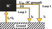 |
| Fig. 3. Current loops around the
conductors inside IC, which become the source of the common
mode (asymmetrical) radiation |
Current and voltage transients related to high frequency switching
and short rise/fall times of useful signals cause EME of digital
ICs. Transients from digital logic spread out as the conductive
signals that may couple onto the power, control and signal lines
and through the IC pins reach the interconnected components on
the PCB. The simultaneous switching of multiple outputs of complex
IC can produce the fluctuations of current and voltage on the
power bus, known under the name of simultaneous switching noise
– SSN.
Current loops around the conductors inside IC, although smaller
than the loops on a PCB, cause the differential (symmetrical)
mode radiation, passing from chip to out-of-package. Unwanted
voltage drops in the circuit and the presence of attached interconnecting
conductors acting as the antennas of various effectiveness, are
the source of common-mode (asymmetrical) radiation. As in the
case of the PCB, this type of emission can be related to the fluctuations
of voltage difference between the PCB reference plane (PCB ground)
and the reference potential USS and supply voltage UDD inside
IC. These fluctuations are called ground and supply bounce, Fig.
3.
The energy carried by emitted electromagnetic waves may be sufficiently
high to induce interfering voltages on the connecting conductors
and cables located around functioning IC. The observed power levels
radiated by some microcontrollers in the frequency band of 1-1000
MHz were in the range of –110 dBm (0.01 pW) to – 75
dBm (about 32 pW). It is rather obvious that the levels of radiated
power can be different for different types of circuits. It is
less obvious that the difference between the circuits of the same
type but coming from various manufacturers or production lines
may be as high as a few tens of decibels. The highest emission
levels are appearing in the vicinity of quartz, clock generator
and output buffers of the circuit. This is the reason for a practical
recommendation not to install in the close proximity of these
networks other electronic components that are particularly susceptible.
Electromagnetic emissions are usually tested in the broad frequency
range from a few kHz up to some GHz. Regarding the complexity
of the emission mechanism, different models and techniques are
adopted as the base of measurement methods.
| Table 1. Basic Features of EME Standard
Test Methods |
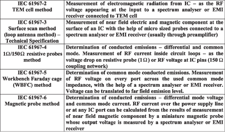 |
Measurement Methods of EME
The International Electrotechnical Commission (IEC) proposed as
the standards five - and practically four - measurement methods
of emission of ICs (elaborated by Working Group 9 of Technical
Subcommittee SC 47A). These are the following methods: TEM cell,
surface scan (magnetic loop), 1 W/150 W (resistive probes), workbench
Faraday cage (WBFC) and magnetic probe. Short characteristics
of the methods are given in Table 1.
These methods together allow evaluation of ICs emission levels
in the frequency range up to 1 GHz, comparison of various types
of ICs, and guide the manufacturer’s efforts to design new
circuits with reduced emission generation. Simplified illustrations
of typical measurement arrangements are given in Fig. 4.
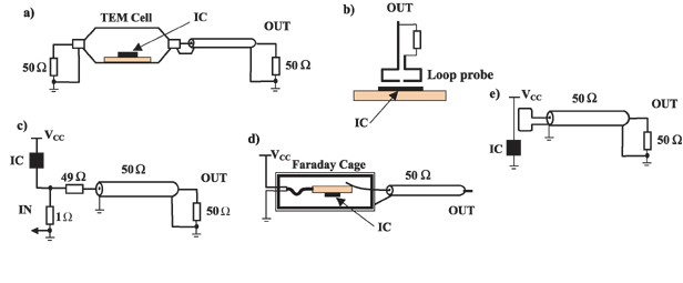 |
| Fig. 4. Simplified illustrations
of typical measurement arrangements: a) TEM or GTEM cell,
b) loop probe for measuring near magnetic fields, c) resistive
probe, d) Faraday Cage, e) magnetic probe |
The radiation level can be measured inside a TEM cell (Fig. 4a),
or a GTEM cell for higher frequencies. The IC is mounted on its
test board that is clamped to a mating port (wall port) cut in
the top or bottom of a TEM cell. The RF voltage appearing at the
input of the connected spectrum analyser is related to the electromagnetic
potential of the IC and its application (test) circuit.
Electric and magnetic components of near electromagnetic field
(roughly at the distance from radiation source less than 1/6 of
the radiated wavelength) can be measured with the help of magnetic
and electric probes (Fig. 4b). The probes are mechanically scanned
over the surface of an IC or other elements mounted on a PCB.
The shift of probes can be done by hand, with the use of a microscope
stage or fully automatically under the control of a computer program.
Automatic equipment provides a two-dimensional picture of the
RF current circulating within the tested PCB. Finally, it can
be easily converted into a coloured map showing the field strength
distribution.
RF emission from small electronic modules or ICs occurs mainly
via the attached conductors and cables. In two of the measurement
methods of conducted emissions (resistive probes, Fig. 4c and
magnetic probe, Fig. 4e), RF current inside the circuit is measured
to allow indirect estimation of the emission level. The variable
RF component of current on the supply lines is dominant and reflects
the whole IC activity in respect to the generation of the electromagnetic
disturbances. The contribution of some I/O ports also should be
taken into account. Thus, spectral characteristics of the supply
current IDD (or ISS) of the IC as well as the selected parameters
of its waveform, defined in the time domain, can be easily correlated
to the emission level. For IC pins that are intended to be connected
directly to long (> 10 cm) PCB traces or cables, RF voltage
measurement using a 150 W coupling network is recommended in IEC
61967-4.
Measurement of common-mode conducted disturbances, produced by
an electronic module or by an IC mounted on its test board, can
be performed inside the workbench Faraday cage (Fig. 4d). This
is a metallic box of 500x300x150 mm, equipped with adequate connectors,
filters and matching elements. RF voltage at the selected IC port
is measured across the used common-mode impedance.
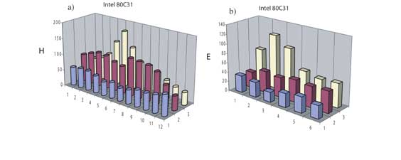 |
| Fig. 5. The distributions of EM fields
over the package of 8-bit Intel 80C31 type of microcontroller:
a) magnetic component, b) electric component |
Illustrative Examples
Digital circuits usually generate the strongest electromagnetic
disturbances. Many experimental results of emission measurements
were obtained for 8-, 16- and 32-bit microcontrollers.
The distribution of magnetic and electric components of the EM
field, measured over the package of 8-bit Intel 80C31 and 8-bit
Dallas Semiconductor DS 87C520 types of microcontrollers are,
respectively, given in Fig. 5 and 6. A DS 87C520 device is pin
and instruction-set compatible to the popular 8051 circuit and
can run at clock rates up to 33 MHz (over 2 times faster than
80C31). Both circuits were mounted on test boards and worked in
the close programming loop that allowed activation of all inherent
blocks. Measurements were performed at the established set of
points over the packages with the help of E and H miniature probes
(made by Langer EM-Technik, Germany). Signals from the probes
were amplified in the broadband amplifier and sent to the input
of a LeCroy 9370 type oscilloscope. Results showed represent the
average peak-to-peak values of the voltages taken from over 100
measurements. As shown in Figures 5b and 6b, the distribution
of the E component is similar in both cases. The highest strength
appears in the vicinity of ICs I/O ports (3rd column, 1-3 rows).
As shown in Figure 5a, the H component for the 80C31 circuit has
its maximum roughly in the same place as the E component. As shown
in Figure 6a for DS 87C520, the H component distribution is more
even, but on average slightly higher. The difference is seen in
the vicinity of I/O port 3 and XTAL terminals (1st column, 9-12
rows).
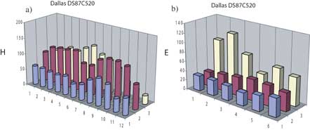 |
| Fig. 6. The distribution of EM fields
over the package of 8-bit Dallas Semiconductor DS 87C520 type
of microcontroller: a) magnetic component, b) electric component |
Even more impressive are the results presented in Fig. 7. Changes
in the design and technology introduced by the manufacturer (Hitachi)
resulted in the substantial reduction (as much as 15 dB) of magnetic
field of the H8S series of microcontrollers in comparison to the
former H8 family. Both circuits are 16-bit microcontrollers with
fclock = 16 MHz.
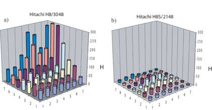 |
| Fig. 7. The distribution of magnetic
component of EM fields over the package of Hitachi 16-bit
microcontrollers: a) H8/3048 type, b) H8S/2148 type |
Examples of the H component distribution over an electronic module
on a PCB, taken with the help of an automatic EMC-Scanner made
by Detectus AB Sweden and an HP 11940A type magnetic probe, are
given in Fig. 8. The four consecutive pictures were taken at four
different peak frequencies: 96, 112, 212 and 631.9 MHz. The change
of localization of the strongest field sources can be easily noticed;
they are related to ICs at lower test frequencies and move to
some output buffers and I/O ports and connectors for higher frequencies.
The above conclusion about the frequency range of the EME of ICs
well correlate with the measurement results obtained, e.g. by
application of resistive or magnetic probe methods. In Fig. 9
the spectral characteristic of an EME of an ST 6210 microcontroller
is presented. The curve, being the envelope of individual spectral
values of the emission, was measured with the help of a magnetic
probe MP-10L (NEC Corp.) that was placed over the IDD supply line
of the circuit (according to IEC 61967-6).
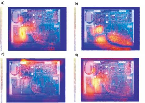 |
| Fig. 8. Distributions of magnetic
component of EM field over electronic module (400x300 mm)
obtained on Detectus AB scanning system; 10 kHz bandwidth,
peak frequency: a) 96 MHz, b) 112 MHz, c) 212 MHz, d) 631.9
MHz (Reproduced with the kind permission of Detectus AB, Malung,
Sweden) |
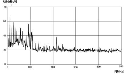 |
| Fig. 9. Spectral characteristic of
ISS current of ST 6210 type microcontroller |
Power supply currents provide valuable information not only on
the conducted emission levels of ICs, but also on their immunity
to external electromagnetic disturbances. On the basis of measurement
and analysis of currents, one can draw conclusions about the disturbance
type and its intensity. Disturbing electromagnetic signals are
revealed in the supply currents much earlier than in any changes
in circuit output signals. Fig. 10 and Fig. 11 show, respectively,
the output voltage and a part of the spectral characteristic of
the supply current of an 80C31 type microcontroller, when a sinusoidal
10 MHz disturbing signal was coupled to the input terminal of
the circuit. It is easy to note the appearance of a fundamental
component of the disturbing signal V1 inside the spectral characteristic
of the IC. Note that there is no evidence of the presence of a
disturbing signal on the IC output voltage. (The visible small
fluctuations are caused by the clock signal.) The situation would,
of course, change if the disturbing signal levels were significantly
higher and sufficient to cause the switching of the IC output.
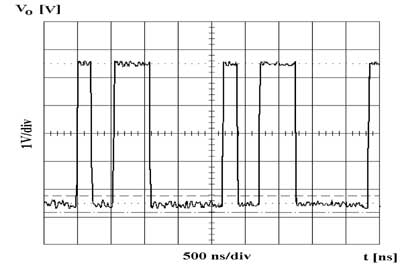 |
| Fig. 10. Output voltage of 80C31
type microcontoller - 10 MHz sinusoidal signal was coupled
to the input port |
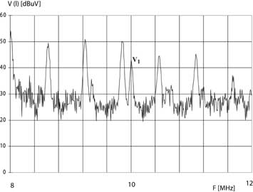 |
| Fig. 11. Selected part of the spectral
characteristic of 80C31 type microcontroller at the conditions
as above, V(I) - voltage at the output of magnetic probe) |
Summary
Integrated circuits and various electronic components inside electronic
modules mounted on PCBs are the source of electromagnetic emissions
that appear as conducted and radiated electromagnetic disturbances
over a broad frequency range. There is a need to measure the emission
levels and quantitatively characterise emission sources. Among
the elaborated and accessible measurement methods worth noticing
are the methods related to the measurement of power supply currents,
since they can reflect the inherent functional activity of the
circuits. EMC
References
[1] IEC 61967 Integrated circuits. Measurement of electromagnetic
emissions, 150 kHz to 1 GHz. Parts 1-6
[2] J.F.Kolodziejski, J. Szczesny: Electromagnetic disturbances
produced by digital integrated circuits (in Polish), Elektronizacja
nr 10, 2002, pp. 21-23
 Jerzy
F. Kolodziejski received his M Sc degree from the Wroclaw Technical
University in 1959, his Ph D (E.Eng.) from the Warsaw Technical
University in 1965, and his D Sc from the Institute of Electron
Technology Warsaw in 1992. He has been employed at the Institute
of Electron Technology since 1970 and as a Full Professor since
2001. For several years, he has been involved in the measurement
methods of semiconductor devices and their reliability testing.
His current interest is in EMC problems, mainly on the IC and
PCB level. He is a nominated expert of the Polish Standardization
Committee and currently is an active member of WG9 SC 47A of the
IEC. He is an author or co-author of a many publications on EMC
problems, including one book (in Polish).
Jerzy
F. Kolodziejski received his M Sc degree from the Wroclaw Technical
University in 1959, his Ph D (E.Eng.) from the Warsaw Technical
University in 1965, and his D Sc from the Institute of Electron
Technology Warsaw in 1992. He has been employed at the Institute
of Electron Technology since 1970 and as a Full Professor since
2001. For several years, he has been involved in the measurement
methods of semiconductor devices and their reliability testing.
His current interest is in EMC problems, mainly on the IC and
PCB level. He is a nominated expert of the Polish Standardization
Committee and currently is an active member of WG9 SC 47A of the
IEC. He is an author or co-author of a many publications on EMC
problems, including one book (in Polish).
 Juliusz
Szczesny received his M Sc degree in physics from the Nicolaus
Copernicus University in Torun, in 1973, and his Ph D from the
Institute of Electron Technology Warsaw in 1987. From 1974 to
1999, he worked on microwave measurement methods and the design
of discrete semiconductor devices. Since 2000, he has been working
on EMC compatibility problems, mainly on ICs and PCBs. He is a
member of WG 2 SC 47E of the IEC as an expert in discrete semiconductor
devices. He is an author or co-author of several publications
on microwave semiconductor devices and EMC problems.
Juliusz
Szczesny received his M Sc degree in physics from the Nicolaus
Copernicus University in Torun, in 1973, and his Ph D from the
Institute of Electron Technology Warsaw in 1987. From 1974 to
1999, he worked on microwave measurement methods and the design
of discrete semiconductor devices. Since 2000, he has been working
on EMC compatibility problems, mainly on ICs and PCBs. He is a
member of WG 2 SC 47E of the IEC as an expert in discrete semiconductor
devices. He is an author or co-author of several publications
on microwave semiconductor devices and EMC problems.
 Practical
Papers, Articles and Application Notes
Practical
Papers, Articles and Application Notes