 |
BOB ROTHENBERG |
Practical
Papers, Articles
and Application Notes
|
BOB ROTHENBERG |
This column is devoted to articles, papers or application notes which would be of interest to EMC practitioners as opposed to EMC academicians. Ideally, such papers should be about 1-3 Newsletter pages in length. If editing for length is required, it will only be with the author's concurrence. Please submit in double-spaced form, as hard copy, disk or e-mail (see page 3 for address, fax and e-mail info).
Digital Clock Transmission Lines and Terminations on Printed Circuit Boards — Part II
by Lee Hill, Silent Solutions (Hollis, NH)
INTRO:
In my view, the sharing
of knowledge gained from experience is an important responsibility of all professional
engineers. In fact, this responsibility is a major reason for the existence of the IEEE
EMC Society. And this column in the Society’s Newsletter is one of the many
opportunities for you to share some of your knowledge. As its title suggests, anything
from a short paper to an application note is appropriate for these pages. If editing is
required, it will only be with the author’s concurrence.
This issue’s contribution is the second part of an article on PCB signal integrity by Lee Hill of Silent Solutions (Hollis, NH). Part I appeared in the last issue of the Newsletter. Lee served as an IEEE EMC Society Distinguished Lecturer from 1992-1994, and received the Society President’s Memorial Scholarship in 1993. He holds an MSEE from the University of Missouri-Rolla.
 |
| Figure 1: Simple PC board circuit model |
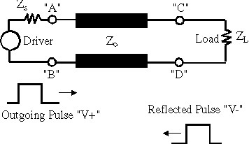
In the first part of this article (see the Winter 1998 issue of the IEEE EMC Society Newsletter), we reviewed the motivation of EMC and digital design engineers to maintain good signal integrity in high speed digital systems. In addition, we discussed a simple qualitative and quantitative method to determine the relative length of a digital transmission line, and thus determine whether or not we should add termination components to ensure that signals on the line will look “nice” in the time and frequency domains. In this article we will examine the nature of signal reflections on digital clock transmission lines, and the termination components and methods used to control them.
As shown in Figure 1, a typical PCB digital clock circuit consists of a driver, transmission line, and load. Here we will consider only circuits that have one driver, and one or more loads. A summary of good digital transmission line design, and the rest of this article for that matter, goes likes this: We would like the signal on the PCB trace to “crash” into a resistor of value Zo either at the source or at the load? The signal is launched from the driver, the signal tells the load what to do, and then its associated energy is absorbed either at the load or at the source. If not, signal energy will bounce back and forth between the source and the load with a frequency equal to 1/(length of line/propagation velocity). If this happens, we will have lousy signal integrity, poor system reliability, and heaps of radiated EMI.
Real Digital Circuits Today
Today’s high performance CMOS clock drivers have the capability to drive a five volt digital signal into loads in excess of 50 pF, while maintaining signal edge rates close to one nanosecond! At this edge rate, we know that we must expect to observe transmission line behavior if the signal trace is only five centimeters (or more) in length. “Transmission line behavior” is microwave engineer talk that means “look out for signal reflections” at both ends (the source and load) of the PCB trace. A well designed circuit will allow no reflections at all, or at most a single reflection at the load, which subsequently will be absorbed at the source.
What Happens on the Transmission Line
In a world without perfectly matched and EMI-quiet transmission lines, we should observe the following: 1) The signal is launched from the driver onto and down the transmission line as an “outgoing pulse” V+. 2) As the pulse travels down the line, the amplitudes of the outgoing traveling voltage and current waveforms satisfy the relationship Zo = V/I, the characteristic impedance of the transmission line. Since digital circuits usually convey information by propagating a time-changing voltage level, we can see that the higher the impedance of the line, the less current (and power) the driver will have to supply. Conversely, lower impedance lines will require more current and more power to propagate a digital pulse at a given voltage level. 3) When the pulse arrives at the load, a “reflected pulse”, V-, will be generated if the impedance of the load does not match the impedance of the transmission line. If we want to know the size and polarity of the reflected pulse, we can define and evaluate a reflection coefficient G at the load as:
G = (ZL- ZO) / (ZL+ ZO)
The amplitude of the reflected wave is then
V- = GV+
The “load” for a digital clock is usually a clock input pin of a high impedance integrated circuit. IC datasheets usually characterize a single input pin to be the equivalent of a five picofarad capacitor. Suppose we are driving a 25 MHz clock signal down a 50 ohm line to a single load at the end of a “long” trace. Do we get a reflection? As just stated, a reflection will be generated if the load impedance does not match the trace impedance. To answer this question, we must calculate the impedance of the load at the highest frequency component of the pulse that we think is “important” or “non-trivial”. Experienced EMC engineers may give a knee-jerk reaction and say “the tenth clock harmonic is the highest frequency that I will ever consider to be important”. Others may resort to a bandwidth rule-of-thumb that equates an upper signal bandwidth equal to 1/(p * risetime). Using both these ideas for the given signal, we get 25 MHz * 10 = 250 MHz, or 1 / (p * 1 nanosecond) = 318 MHz. To remain employed, let’s be careful and pessimistic, and choose the higher of the two results, 318 MHz. The load impedance is that of a five picofarad capacitor (Z = 1/(wC) calculated at 318 MHz, equal to 1/ ( 2 * p * 3.18 E+08 * 5 E-12) = 100 ohms. The load impedance ZL (100 ohms) is not equal to the given line impedance Zo (50 ohms), and therefore a reflected pulse “V -” will be generated.
 |
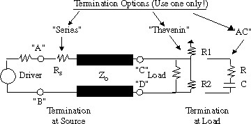
| Figure 2: Transmission line with termination components |
If we want to dramatically reduce the amplitude of the load reflection, we can add one or more termination components at the load to force the impedance at the end of line to equal approximately 50 ohms, the PCB trace characteristic impedance Zo, in our example. As shown in Figure 2, we generally have a choice of two termination configurations at the load: 1) Two resistors that comprise a voltage divider with a Thevenin equivalent impedance (R1 in parallel with R2) of Zo, or 2) A series resistor and capacitor combination with R = ~Zo, and C = ~ 102 pF. Configuration “1” is often referred as a “Thevenin” termination; “2”, an “AC” termination. The Thevenin termination makes the driver work much harder at low frequency harmonics, since a high impedance, “light” load will be swamped by a shunt resistance of 45 to 70 ohms to match the Z of a modern digital PCB. Note also that the “Thevenin” termination consumes real DC power. The “AC” termination eliminates DC power consumption and reduces low frequency harmonic loading by making the termination resistor R “appear” in the circuit only at higher frequencies, where the capacitor’s impedance is comparable to or less than the impedance of the line.
In the event that there is more than one capacitive load at the end of the line, we may be able to model all the loads together as a single lumped capacitance. Beware of “heavy” capacitive loads where the equivalent load impedance is much less than the line impedance. In such circumstances, a “Thevenin” or “AC” termination that appears in parallel with the load cannot be used, since it can only reduce the aggregate load impedance. A too-low load impedance resulting from heavy capacitive loading might actually require additional series impedance to increase the aggregate load impedance to that of the line impedance Zo.
Instead of using a load termination to prevent the generation of a reflected pulse at the load, many digital circuits use a series termination resistor at the source (also shown in Figure 2). In this case, the outgoing pulse that is launched down the line is reduced in amplitude by the voltage divider formed by the series resistor and the characteristic impedance of the line;
V+ = VAB * (Zo)/(Zo + Rs).
Now we depend upon the positive reflection that occurs at the light capacitve load to “bounce up” the load voltage to an acceptable digital threshold. The value of series resistor is usually chosen to be approximately (Zo - Zs), so that when the reflected pulse V- arrives back at the source, it “sees” Zs + (Zo - Zs), or just Zo. When using a series terminator for extremely fast and strong drivers (i.e., Rs very small), the terminator resistance must approach Zo. The outgoing pulse voltage V+ then will be attenuated by as much as one-half the source voltage VAB. In such cases, the outgoing pulse voltage may be so small that the reflection at the load is required to cause the load to reliably change state. If we try to add additional loads between the two ends of a transmission line with series termination, we may not be able to reliably switch these devices in a predictable manner, since the outgoing pulse is so small and the reflected pulse is heavily dependent upon the source edge rate and characteristics of the load. IC application notes wisely warn us about the perils of using series termination methods in conjunction with heavily loaded lines with distributed loads.
 |
| Lee Hill may be contacted at Silent Solutions EMC Consulting20 Patch RoadHollis, NH 03049tel: 603.465.3920e-mail: noiseless@aol.com |
Return to Contents page