 |
Figure 1. Sketch of the three-layer shield. |
Maria Sabrina Sarto1, Sergio Di Michele2, Peter Leerkamp2, Henk Thuis2
1 University of Rome
"La Sapienza",
Dept. of Electrical Engineering, via Eudossiana 18,
00184 Rome, Italy
e-mail: sarto@elettrica.ing.uniroma1.it
2 Stork Screens B.V.,
Raamstraat 1-3,
5831 AT Boxmeer, The Netherlands
e-mail: peter.leerkamp@stork.com
The design and realization of lightweight shields to reduce radiated emissions and electromagnetic interference (EMI) with sensitive electronic apparatus and systems is a challenge for electromagnetic compatibility (EMC) engineers.
Techniques that are currently used to improve the shielding performances of light materials such as plastics and composites are: the insertion of conducting meshes in the substrate [1, 2], the use of conducting additives and fillers prior to injection molding [3, 4] and the use of conducting coatings [5-8]. Among these techniques the use of conducting coatings allows the realization of lightweight shields.
The purpose of this paper is to demonstrate that thin coatings of conducting material, having thickness of a few micrometers, can provide good shielding performances in the radio-frequency range, up to a few gigahertz. The deposition of such coatings on polycarbonate foils leads to a new concept of lightweight thermoformable shield, which can be used to reduce EMI from and against printed circuit boards (PCBs) in electronic devices.
Applications of the innovative shielding concept are in different fields, when the requirement of light weight is a stringent constraint in the design of the shields. Examples are: portable electronic devices (PEDs) such as cellular phones, walk-talkies, portable radios and CDs, equipment to be used or installed onboard aircraft, on satellites, etc..
|
Figure 1. Sketch of the three-layer shield. |
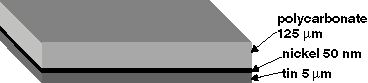
The new shield is made by a polycarbonate foil having the thickness of 125 µm, which is coated by a 50-nm thick layer of nickel and a 5 µm-thick layer of tin, as sketched in Fig.1.
The choice of the polycarbonate as substrate is suggested by its thermoforming properties. Moreover, among thermoplastics, it presents a relative high molding temperature (approximately 200°C).
The choice of tin was suggested by its mechanical properties. Tin is a very ductile metal, and is also characterized by good resistance against corrosion and aging. The 5µm-thick layer of tin is realized by electroplating. Such technique allows the manufacturing of very compact coatings, is rather inexpensive and fast, and is suitable for deposition of coatings over wide-surfaces. One limitation of the technique is that it can be applied to realize only metallic coatings over conductive substrates: therefore the tin-layer cannot be deposited by electroplating directly on the polycarbonate foil.
In order to overcome such limitation, a thin layer of nickel, having the thickness of only 50 nm, is deposited first on the polycarbonate substrate by DC magnetron sputtering. The magnetron sputtering technique is a vacuum deposition technique which has the advantage, with respect to electroplating, of allowing the realization of conductive coatings, on both metallic and non-metallic substrates. It also allows the realization of very compact coatings, and permits a fine control of the thickness growth of the film. However, the DC magnetron sputtering has two main drawbacks: it is only suitable for very thin coatings (with thickness not higher than 1 µm); and it is also generally more expensive than electroplating.
The choice of nickel was suggested by its chemical properties: in particular, it is not subjected to oxidation and it does not react with tin or polycarbonate. Moreover, it has good adhesion properties on plastic substrates.
The thickness of 50 nm was the minimum one resulting from the compromise of reducing the sputtering deposition time, and of realizing a conductive substrate which is able to guarantee correct deposition of the tin layer by electroplating.
Finally the metalized foil is thermoformed at the temperature of 200şC to realize lightweight shielding covers and caps, having whatever shape. Figure 2 shows some examples of lightweight shields.
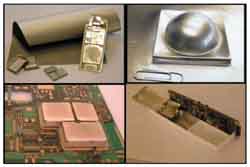 |
Figure 2. Examples of thermoformed shields. |
Mechanical, chemical and aging tests have been performed in order to characterize: the thickness profile of the metallic layers after thermoforming; the adhesion and abrasion properties of the coating, the electrical conductivity before and after exposure to a damp environment and the effect of aging on the metallic layers [9].
The shielding performances of planar and 3-D samples of metalized polycarbonate foils before and after thermoforming have been tested experimentally in a wide frequency range, and considering different set-ups.
1) The planar samples. The planar samples before thermoforming have been tested by using the standard ASTM 4935D set-up [10]. The ASTM 4935-D test method is probably one of the most used and reliable way to characterize the shielding performances of planar samples. It provides the shielding effectiveness of the material against a TEM wave in a coaxial cable, in the frequency range from about 30 MHz to a few gigahertz. These frequency limits are not exact but are based on the decreasing of displacement currents due to decreased capacitive coupling at lower frequencies, and on overmoding (i.e. excitation of modes other than the TEM) at higher frequencies.
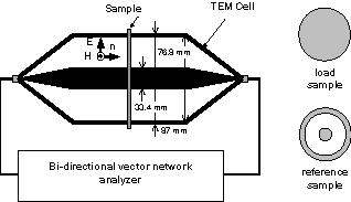 |
Figure 3. Schematic representation of test set-up for the SE measurement of planar samples, with the load and reference specimens. |
The test set-up, sketched in Fig.3, is composed by: the bi-directional network vector analyzer, the 50-W-coaxial waveguide, the load test specimen and the reference one and double shielded coaxial cables. The two parts of the TEM coaxial waveguide are not electrically connected, but are coupled through the sample. The SE in decibels of the sample under test (load specimen) is defined by:
![]() (1)
(1)
in which ![]() is the transmission coefficient measured
when the reference sample is mounted inside the waveguide, and
is the transmission coefficient measured
when the reference sample is mounted inside the waveguide, and ![]() is the transmission coefficient measured with the load sample. Such a test
procedure allows one to cancel the effect of the contact resistance between the sample and
the metallic waveguide; therefore, it is very important that the surfaces of both the
reference and load specimens are properly treated before the test.
is the transmission coefficient measured with the load sample. Such a test
procedure allows one to cancel the effect of the contact resistance between the sample and
the metallic waveguide; therefore, it is very important that the surfaces of both the
reference and load specimens are properly treated before the test.
Even though this method allows a high accuracy and reproducibility of the measurements, it has two main drawbacks: it can be used to test only planar samples and the frequency range is limited between about 30 MHz and 1.5 GHz, in order for the cell to work in the TEM mode.
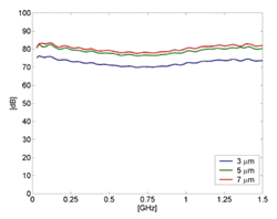
Three different thicknesses of the tin layer have been considered (i.e. 3 µm, 5 µm, 7 µm) in order to assess the influence on the shielding effectiveness (SE) of the coating thickness. The measured data are reported in Fig.4: the average SE in the considered frequency-range is about 72.5 dB for the shield with the 3 µm-thick-coating, nearly 79 dB for the sample with the 5 µm-thick-coating, and 80.5 dB for the shield with the 7 µm-thick-coating.
 |
 |
|
Figure 4. Frequency spectra of the measured SE of planar samples having thickness of the tin layer of 3 µm, 5 µm, 7 µm. |
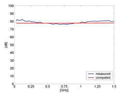
Figure 5. Frequency spectra of the measured and computed SEdB of the planar sample having thickness of the tin layer of 5 µm. |
The obtained results are in good agreement with the values of the SE that are calculated by applying the theoretical expressions valid for a multilayered panel illuminated by a plane wave [9,11]. Table I shows the values of electrical conductivity, relative permittivity, relative permeability, and thickness of tin, nickel and polycarbonate used in the simulations.
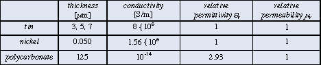 |
Table I. Electrical conductivity, relative permittivity, relative permeability, and thickness of the tin, nickel and polycarbonate layers. |
The obtained numerical and experimental results are summarized in Table II, where the average values of SEdB, in the frequency range from 30 MHz to 1.5 GHz, are reported. As an example, Fig.5 shows the measured and computed frequency spectra of SEdB for the planar sample with the 5 µm-thick layer of tin.
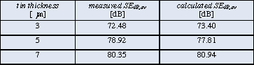 |
Table II. Measured (ASTM 4935D) and calculated SEdB of the three-layer planar sample for different values of the tin-thickness. Average values in the frequency range from 30 MHz to 1.5 GHz. |
It should be observed that numerical experiments have also demonstrated that the effect on the SE of the presence of the polycarbonate foil is absolutely negligible in the considered frequency range, due to the high resistivity and small thickness. Moreover, the presence of the nickel layer affects the SEdB of less than 1 dB, because it is thin compared with the tin one.
Therefore, theoretical analyses are carried out in order to ascertain the influence on the SE of the EM-wave reflection and absorption phenomena as regards a single layer of tin, illuminated by a TEM plane wave in the frequency range up to 1.5 GHz.
For a single layer indefinite shield, SEdB can be expressed in the following form [12]:
![]() (1)
(1)
in which:
![]() (2)
(2)
is the reflection coefficient at the air/metal interface,
![]() (3)
(3)
is the absorption coefficient, and
![]() (4)
(4)
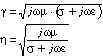
is the coefficient accounting for the multiple reflections inside the shield [N.B.: the approximate expressions are only valid using SI-Units (International System of Units)]. In eqs.(2), (3) and (4), d is the shield thickness, µr the relative magnetic permeability of the shield, f the frequency, sCu=5.8×10⁷ S/m the electrical conductivity of copper, h0 the free-space impedance, g and h are respectively:
 (5)
(5)
where s is the electrical conductivity; e and m are the electrical permittivity and the magnetic permeability of the material realizing the shield; w is the angular velocity.
Table III reports the values of RdB, AdB and BdB for the tin layer alone, considering the different thicknesses of 3 µm, 5 µm, 7 µm, at the frequencies of 100 MHz, 1 GHz, and 1.5 GHz. Notice that in all cases the reflection phenomenon plays a dominant role in the EM shielding. However, for frequencies higher than 1.5 GHz, the absorption coefficient becomes more and more important since it grows up as the root of f.
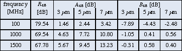 |
Table III. Calculated reflection, absorption, and multiple-reflection coefficients of a single layer of tin (s=8×10⁶ S/m), for different values of thickness. |
2) The thermoformed shield. The SE of the thermoformed shield has been tested in the anechoic chamber of the National Aerospace Laboratories (NLR) in The Netherlands. To this purpose the simple cover, having the geometrical configuration sketched in Fig.6, is used. The tin layer has a thickness of 5 µm.
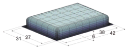 |
Figure 6. Sketch of the shielding cover used in the far-field and near-field tests inside the anechoic chamber (dimensions in mm). |
Both far field and near field test configurations have been considered. In the far field set-up the incident plane wave is produced by a horn antenna in the frequency range from 1 GHz to 2 GHz, located at 1.5 m far from the shield. In the near-field set-up a small loop antenna is printed on a board and supplied with power through an amplifier in the frequency range from 1 GHz to 2 GHz. The experimental configurations are sketched in Figs. 7 (a) and (b).
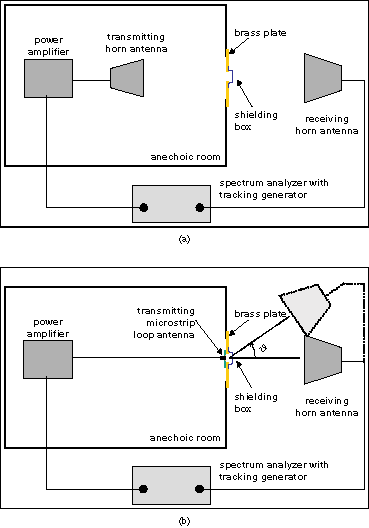 |
Figure 7. Schematic configuration of the test-set up for the far-field (a) and near-field (b) measurements. |
 |
 |
|
Figure 8. Frequency spectra of the SE measured in the Far-field and Near-field tests: (a) mean and (b) standard deviation among different measurements made on several cover shields having the same characteristics. |
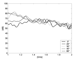
Figure 9. Frequency spectra of the SE measured in the near-field test, with respect to different angular positions of the receiving antenna. |
In order to assure a good contact between the borders of the shield and the reference ground, the shield is pressed against the brass plate by means of a pressing device which is made entirely of polyacrylate, so that it is expected that its influence on the experimental results is negligible.
The measurements are made on different samples in order to verify the repeatability of the results. In fact, the measurement is affected by uncertainty due to several aspects: resonances inside the anechoic chamber, coupling between the near-field source and the shield, and dynamic range of the measurements limited by the quality of the room.
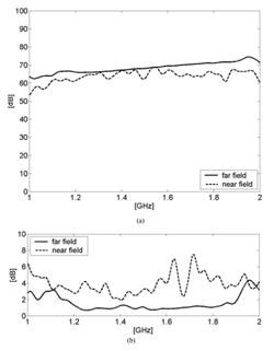
The frequency spectra obtained by the average of several SE measurements made on different samples having the same characteristics, in the far and near-field test set-ups, are reported in Fig. 8(a). The corresponding standard deviations are shown in Fig. 8(b).
It can be observed that in the far-field tests the measured mean varies from about 63 dB at 1 GHz to nearly 70 dB at 2 GHz. The corresponding standard deviation is 1 dB - 1.5 dB from 1.2 GHz to 1.8 GHz; higher values of standard deviation at the boundaries of the investigated frequency range are probably due to the worst performances of the radiating and receiving antennas nearby 1 GHz and 2 GHz.
In the near-field configuration, the SE of the shielding caps is reduced by about 5 dB - 10 dB with respect to the far field set-up. Moreover, it is noted that the near-field measurements are much more noisy than the far-field ones, and that the standard deviation is higher (between 2 dB and 7 dB): this behavior is probably due to the combined effects of the mismatching between the amplifier and the radiating loop antenna, and loop resonances.
Finally, the sensitivity of the SE against variation of the angular position J of the receiving antenna in the near field set-up is analyzed (Fig. 7(b)). The obtained experimental data are reported in Fig. 9: the zero-degree configuration corresponds to the case in which the magnetic loop and the receiving antenna axes are parallel. In the test, the distance between the shielding box and the receiving antenna is kept constant. It is interesting to note that in the high frequency range the SE is weakly influenced by the position of the receiving antenna. At frequencies lower than 1.4 GHz the J = 0° configuration represents the worst case as regards the SE. In fact, for higher values of J the coupling between the loop source and the receiving antenna through the aperture is weak.
An innovative concept of lightweight shield is described. The proposed shield is made by a thermoformed polycarbonate foil, which is coated by a thin layer of tin before thermoforming. Due to the great formability of polycarbonate and to the good ductility of tin, the shielding foil can be used to realize covers and caps, having different shapes, to be mounted on PCBs in order to reduce EMI and radiated emissions.
It is demonstrated that a metallic coating of only 5 µm of tin can provide an average shielding effectiveness against plane wave of about 79 dB in the frequency-range from 30 MHz up to 1.5 GHz. Such performance is motivated by the fact that in the considered frequency range the shielding phenomenon is dominated by reflection of the EM wave at the air-coating interface: for instance at 1.5 GHz the percent ratio between the reflection coefficient (RdB) and the shielding effectiveness (SEdB) is 87%, whereas the percent ratios between the absorption coefficient (AdB) and the multiple reflection coefficient (BdB) and SEdB are 12% and 1%, respectively. Therefore it can be concluded that even very thin layers of conducting material are able to produce a strong attenuation of the incident field.
Near field and far field measurements performed in an anechoic chamber, in the frequency range from 1 GHz to 2 GHz, have demonstrated that the average SE of the thermoformed shields varies between 60 dB Đ 75 dB in spite of the non-uniform thickness distribution produced by the thermoforming process. Nevertheless, it should be highlighted that such values of shielding effectiveness are obtained as regards shields without seams or apertures, and that the metallic coating is continuous over the surface of the polycarbonate foil.
The developed shielding covers have been designed to be mounted on PCBs inside cellular phones. The main advantages of the proposed solution are the low cost of production and installation, and the light weight.
Maria Sabrina Sarto received the Ph.D. in Electrical Engineering in 1997, and since 1998 has been Associate Professor of Electrical Engineering at the University of Rome "La Sapienza", where she teaches the course of "Basic Electrical Engineering" for the degree in Aerospace Engineering, and is the head of the EMC Laboratory of the Department of Electrical Engineering. Professor Sarto is the author of more than 70 technical and scientific papers published in International Journals and in the Proceedings of International Symposia, covering several EMC topics. In particular, her research interests include susceptibility and radiated emission of transmission line networks, electromagnetic characterization of composite materials and thin films, lightning interaction to aircraft, and numerical modeling. She received the Best Paper Award at the 1993 IEEE International Symposium on EMC, in Dallas, Texas, the President's Memorial Awards in 1996 and 1997, the 1997 Best Transactions on EMC Paper Award, and the Best Poster Paper Presentation Award during the International Symposium EMC EUROPE 2000 in Brugge. She is Associate Editor of the IEEE Transactions on Electromag-netic Compatibility, a member of the TC9 Committee on numerical modeling in EMC, and of the IEEE STD 299 working group. Professor Sarto is a Senior Member of the IEEE and a Distinguished Lecturer of IEEE EMC Society.
 |
Sergio Di Michele was born in Campobasso, Italy, in 1976. He received his degree in Electrical Engineering in 2000 from the "University of Rome Đ La Sapienza". In November 2000 he joined Stork Screens as a researcher. His research activities are focused on electromagnetic shielding, in particular on the shielding properties of composite materials.
 |
Peter Leerkamp graduated in Physical Chemistry at the University of Leiden, the Netherlands. For more than ten years he worked at Stork Screens in the field of research and development; his main topics being sputtering, electroplating, electroforming and photo-etching. Now he works in the New Business Development department of Stork Screens, focusing on market introduction and market acceptance processes of new products in the market.
 |
Henk Thuis received his Ph.D. in Molecular Physics at the University of Nijmegen, the Netherlands. In 1980 he joined the Stork Group, where he still works. During these years he dealt with product development and was product manager for digital engraving and printing products in the textile market; since 1999 he is involved in the development of shielding products at Stork Screens. EMC