Welcome to this new section of the EMC Newsletter! “Design
Tips” will be brought to you in each issue to further
your education on the practical side of EMC. There is a lot
of very good accumulated knowledge about EMI/EMC design within
our community. This new section is intended to help people
share this knowledge with everyone else, without the need
for submitting a formal paper. The goal is to have a short
(1-2 pages) description of different design tips followed
by a “real world” example that could be useful
to others in the EMC community. But, this means I’ll
need your help! Please send me your most useful design tip
for consideration in this section. Ideas should not be limited
by anything other than your imagination! Please send these
submissions to bruce.arch@ieee.org.
I’ll look forward to receiving many Design Tips! Please
also let me know if you have any comments or suggestions for
this section, or comments on the Design Tips articles. This
first Design Tip concerns one of the most misunderstood concepts
within EMI/EMC design….”GROUND”.
Editor’s Note: Many thanks to EMC Board of Directors
Member, Elya Joffe, and his Membership Development Task Force
Committee, who suggested creating a “Design Tip”
section of the Newsletter to enhance member benefits. Thank
you too to Dr. Archambeault for his willingness to coordinate
these articles as our newest Associate Editor. |
Electrical engineers are quite familiar with
schematic drawings. While the schematics are accurate for the
intended signal flow, there is a very important piece of the signal
path missing! The signal voltages are usually all referenced to
“ground”, and the schematic assumes that all these
signals have a common reference point. However, this is not true
for high-speed signals.
The concept of “ground” requires that a large area
(PCB or metal chassis, for example) be at the same potential/voltage.
At low frequencies (for example in the audio frequency range)
this is easily achievable, and the concept of ‘ground’
has definite meaning. However, at today’s high speed data
rates, the frequency content of the signals is significantly higher,
resulting in wavelengths that are much smaller than the ‘ground’
area we use. This results in a voltage difference across the ‘ground’
plane (or chassis) and makes the concept of ‘ground’
at high frequencies completely meaningless. When dealing with
high frequency signals, it is important to remember, “Ground
is a place for potatoes and carrots”! There
is no magic about ‘ground’…it is simply a possible
current path.

The important point is that for EMI/EMC we need to consider the
current, not the voltage, in our signal paths. Since current must
always flow in a loop back to its source, the return current path
must be considered as well as the intended signal path along a
PCB trace. Any interruptions to the return current path can have
serious negative effects to the EMI/EMC performance of a PCB.
A very slight deviation in return current path can result in enough
inductance to dramatically increase emissions.
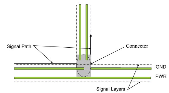 |
| Figure 1. Initial Two Board Configuration |
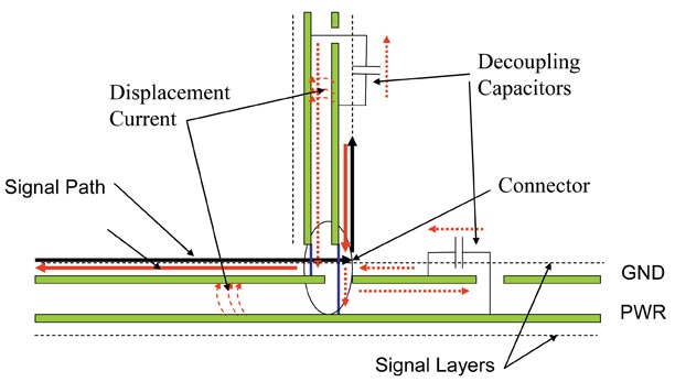 |
| Figure 2. Return Current Paths for
Initial Configuration |
The return current path is also very important when considering
mother/daughter board configurations. Figure 1 shows a simple
4-layer board example of a mother/daughter board configuration
and a signal path from the motherboard to the daughter card through
a connector. If we consider how the return current will flow from
this configuration, we should expect that the return current would
spread out to include displacement current through the dielectric
between GND and PWR as well as local decoupling capacitors (depending
on their distance and the plane separation). Figure 2 shows the
return current for this configuration. The added return current
path length results in additional inductance in the total path,
resulting in a ‘noise’ voltage between the two GND
planes (across the connector). This noise voltage will drive the
wide, thin, monopole-like antenna, resulting in increased emissions.
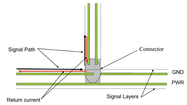 |
| Figure 3. Improved Return Current
Design |
However, if we had simply considered the return current path and
routed the signal trace so that it was referenced to the same
plane (PWR or GND), the return currents are able to stay close
to the signal trace (Figure 3), and emissions are greatly reduced.
When we consider the return current path, more ‘ground’
is not always the ‘right’ answer! For example, on
a recent design, there was a 144-pin connector with many high-speed
signals traveling from one board to the other. It was determined
that 30 pins could be used for ‘power’ and ‘ground’
combined. At least five pins must be ‘power’ so there
would not be an excessive DC voltage drop across the connector.
How many of the remaining 25 pins should be ‘ground’?
In this particular design, it turned out that about 2/3 of the
total signal pins were referenced to the ‘power’ plane,
and only 1/3 referenced against the ‘ground’ plane.
This meant that of the total 30 possible power/ground pins, 2/3
should be ‘power’ and only 1/3 should be ‘ground’!
More ‘ground’ pins was NOT the best design for this
case. Of course, once we consider both the ‘power’
and the ‘ground’ pins to be return current paths,
it is obvious we should distribute them throughout the signal
pins to keep the return current deviation as small as possible
(compared to putting all the ‘ground’ pins at the
ends of the connector, etc.).
The ‘ground’-to-‘ground’ noise voltage
is very real. A simple differential voltage measurement between
the ‘ground’ layer on a motherboard to the ‘ground’
layer on a daughter card (in this case a memory DIMM) is shown
in Figure 4. A noise voltage of 0.8 volts peak-to-peak was measured
for a signal strength of 2.5 volts! Nearly 1/3 of the total signal
voltage swing was just ‘ground’ noise. In this example
(Figure 4), no consideration was given to the return current path
and the resulting noise between ground-references on the two boards
was significant.
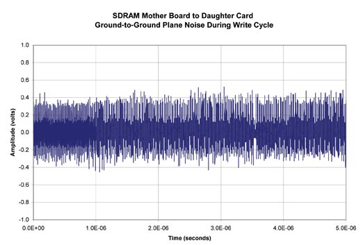 |
| Figure 4. Measured Example of Ground-to-Ground
Noise from Poor Return Current Design |
When we consider the most important concerns for good EMI/EMC
design, the schematic is not as important as the physical layout
of the signal path and the return current. Since today’s
high speed PCBs have many layers and are very complex, it is difficult
for an engineer to examine each critical signal path for a good
return current path. Automated EMC rule checking tools can examine
each net in turn, regardless of the PCB complexity. The key to
selecting an automated rule checking tool is to make sure it can
interface well with your existing design process, it is easy to
use, and it can display rule violations in a graphical and easy
to understand manner.
The most important EMC design rules for high speed PCBs concern
the return current path. Since the return current will always
find a path that minimizes the inductance of that path, the return
current will always flow on the nearest plane, whether it is called
‘ground’ or ‘power’ or ‘carrots’.
When traces cross a split in the return plane (for example, if
a trace is routed next to a power layer with multiple power islands),
the return current’s path is interrupted. Changing layers
within the PCB so that the return current must also change planes
will also interrupt the return current path. Remember, the return
current must always get back to its source. It will get back to
its source. The only question is whether it will be a path that
is beneficial to you, or if it will cause problems. So, “Do
you feel lucky today?” It is always best to design ‘on
purpose’ rather than ‘by luck’. EMC
 Design
Tips: EMC Effects from the Hidden Schematic
Design
Tips: EMC Effects from the Hidden Schematic