
Bob Rothenberg
Associate Editor
Two practical papers are presented in this issue. The first, by Kevin Slattery of Daimler- Chrysler, provides descriptions and comparisons of three measurement techniques for VLSI emissions. The second, by EMC consulting engineer Michel Mardiguian, consists of comments on the article by Ken Javor published in Issue No.180 (Winter 1999).
Members of the IEEE EMC Society are encouraged to submit practical papers and articles for publication in this section of the Newsletter. Maximum length is approximately 1500 words plus 6-8 figures. Submissions may be transmitted via e-mail, fax or snail mail. See addresses on page 3.
Comments from readers are also welcome, either as a letter (or e-mail) to the editor or directly to the authors.
K.P. Slattery
DaimlerChrysler
At the heart of almost every EMI/EMC problem is what to do about the source of emissions. These emissions may be causing problems in the surrounding environment through direct radiated interference; they may be showing themselves indirectly through emissions emanating from the module harness; or they may show themselves by creating functional problems within the module circuitry itself. In all cases, the designer needs a method for identifying and then characterizing these emissions. This paper describes three methods for accomplishing this. It is concerned primarily with emissions generated by VLSI devices such as microprocessors, ASICs and other large scale devices that use high speed clocks. Two of the methods to be described are essentially similar, but differ in the frequency range that they address. The third method is complementary to the first two in that, once having characterized the spectrum of concern, the designer can use this method to investigate the geometry of the emissions at the device package and die level.
The Fischer mini-TEM cell has been available for some time now, and has seen use both by end users of VLSI devices, and by manufacturers of the devices. The frequency range is 10 kHz to 1.5 GHz. The device is described in SAE 1752/3, and in [1]. The basic idea is that the device to be measured is attached to a multi-layer PC board with the device on the side interior to the cell, and all supporting circuitry on the flip side, outside the cell. Because the device can now be considered a part of the cell structure, the device itself does not, to any appreciable degree, perturb the field structure within the cell. One then obtains quite good spectral measurements that can be correlated with OATS and anechoic measurements.
The Lindgren OmniCell is a GTEM structure constructed to perform a measurement similar to the Fischer cell. The Lindgren cell extends the range of the measurement to 7-8 GHz, for correlatible measurements, and to 16 GHz for comparative measurements.
The DaimlerChrysler Surface Scan is a technique for scanning a VLSI device at the package and the die level. Both the magnetic and the electric near fields can be measured. For magnetic measurements, a simple loop fashioned from rigid coax is used and oriented in two orthogonal directions, the resulting data are then combined to arrive at the total magnetic near field. The electric probe is a truncated rigid coax. Both probes are placed to within 100-200 µm of the surface of the device to be measured. 10,000 scan points are typically accumulated at each frequency of interest. This results in scan steps of approximately 70-100 µm. Structural resolution has been determined to be on the order of 100-200 µm. While this cannot resolve individual transistors, it does offer a means for scanning and characterizing functional areas within the device, such as PLL, CPU, memory, A/D, etc. Additionally, the Vdd/Vss topology and related emissions can be measured.
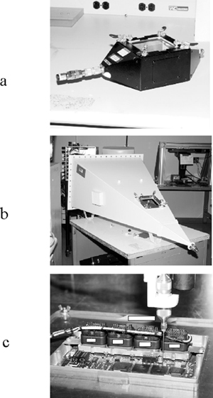
Figure 1. a) Fischer mini-TEM cell b) Lindgren OmniCell c) DaimlerChrysler Surface Scan.
Figure 1 shows the three devices that will be discussed. Figure 2 shows a set of measurements taken in both the mini-TEM and the OmniCell GTEM. The measurements were made using an electrically small electric monopole, and an electrically small magnetic loop. Observation of the resulting plots shows that both devices have a linear response through the range of measurement. However, the GTEM is clearly more monotonic than is the mini-TEM above 1200 MHz. Equally obvious is that either device can be used in the range 100-1200 MHz without any fear of one device giving a set of data different from the other device.
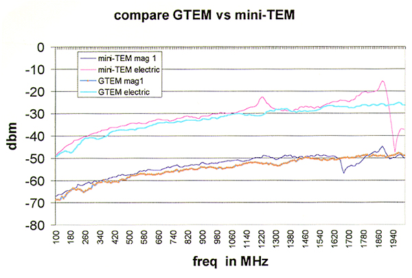
Figure 2. A comparison of the mini-TEM and the GTEM, 100-2000 MHz, electric and magnetic field.
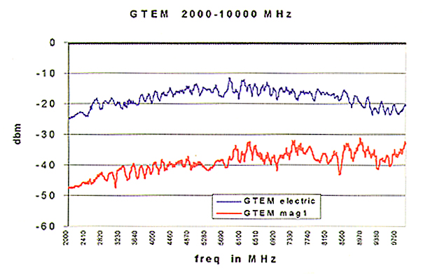
Figure 3. The GTEM, over the range 2000-10000 MHz, electric and magnetic field.
Figure 3 shows the measured data, using the same electric and magnetic probes, for the GTEM through 10 GHz. The GTEM is seen to be monotonic through approximately 7 GHz, after which the response levels off and then starts decreasing. This effect is assumed (at present) to be due to wall losses in the GTEM becoming predominant. However, it should be noted that the magnetic and electric fields maintain a reasonably constant relationship until 8 GHz.
Figure 4 is a comparison of measurements made in the GTEM, and in the mini-TEM, of a 16 bit microcontroller running at 16 MHz, over the range 500-1000 MHz. Because of the density of spectral components it is difficult to do a point by point comparison of the results. Figure 5 is a plot of the same data sets, but the spectrums have been smoothed using a 16 point moving average.
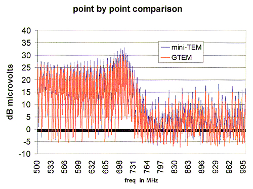
Figure 4. A comparison of measurements taken from a 16 bit
micro- controller, operating
at 16 MHz, mounted on a BGA.
As Figure 5 shows, both devices give approximately the same response. The interested reader is directed to [2], [3] where the mini-TEM cell is discussed in greater detail, and a better appreciation of the cells applications can be gained.
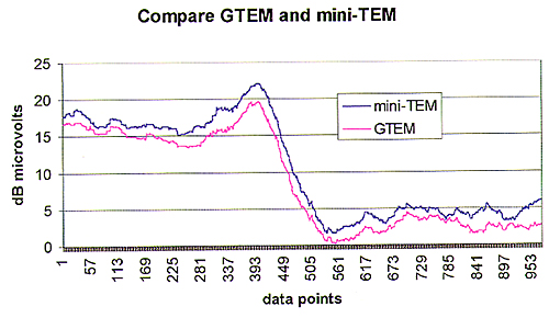
Figure 5. Same measurement as Figure 4. The data has been
smoothed with a moving average
taken every 16 data points for better comparison.
The plots in Figures 6 and 7 show the Daimler-C hrysler Surface Scan images from the same 16 bit micro- controller that was measured in the GTEM and in the mini-TEM cell, scanned at 32 MHz (Figure 6) and 80 MHz (Figure 7).
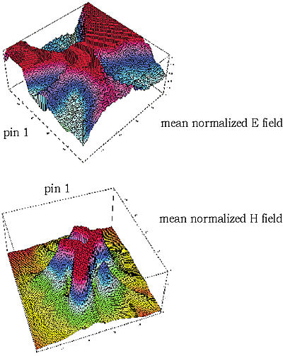
Figure 6. Surface Scan images of a 16 bit microcontroller,
operating at
16 MHz, scanned over the entire BGA package at 32 MHz, magnetic and
electric near field.
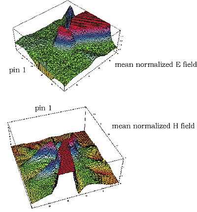
Figure 7. Surface Scan images of a 16 bit microcontroller
operating at
16 MHz, scanned over the entire BGA package at 80 MHz, magnetic and
electric near field.
These images are comprised of 10,000 scan points taken over the surface of the entire BGA package, 17 mm by 27 mm, with the probe at a distance of 150 µm. The peaks have been truncated to better show some of the underlying detail. Notice the differences between the magnetic and electric field distributions at the two frequencies shown. Clearly, the current distributions within the device are markedly different as a function of frequency.
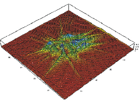
Figure 8. Second derivative of the magnetic field over the 16-bit processor BGA, at 64 MHz.
Figure 8 shows some of the image processing that can be done with the data array generated with Surface Scan. We have taken the discrete array of the measured magnetic field at 64 MHz, imported it to Mathematica, a commercial software package, and generated a continuous function of two variables. We then differentiated this function, arriving at a secondary function related to the magnetic density over the VLSI device. This is shown in the figure. Using this method, further detail within the package, and deep within the die, can be seen. For instance, certain Vdd and Vss pin pairs can be seen to be more pronounced than others. Using this technique on a different device, and working with the manufacturer, we were able to reduce the module level emissions by 8-10 dB by rearranging the functional floorplan and modifying the power and ground feed to the digital core of the device.
By working at the VLSI device level to reduce system and module level EMI, the designer can have a large economic impact on the EMC of a product. By characterizing and mapping the emissions from the dominant source in a module, the EMC engineer may be able to identify and thereby mitigate EMI at the package and die level. By reducing the EMI at the source, EMC fixes introduced at the PCB level may be eliminated, thereby reducing the manufacturing cost and easing the manufacturability of a product.
[1] Investigation of the Theoretical Basis for Using a 1 GHz TEM Cell to Evaluate the Radiated Emissions from Integrated Circuits, Muccioli, North, Slattery, 1996 IEEE International Symposium on EMC, Santa Clara, CA
[2] Measuring the Radiated Emissions From a Family of Microprocessors Using a GHz TEM Cell, Slattery, Muccioli, North, IEEE Transactions on EMC, May 1999, Volume 41, Number 2
[3] Characterization of the RF Emissions from a Family of Microprocessors Using a GHz TEM Cell, Muccioli, North, Slattery, 1997 IEEE International Symposium on EMC, Austin, Texas
 Kevin
Slattery is responsible for Module EMC analysis and testing at DaimlerChrysler
Electronics in Huntsville, Alabama. Previously, Mr. Slattery spent 14 years
at the Stanford Linear Accelerator Center, designing high speed timing electronics
and particle transport systems. He can be reached via e-mail at kslattery@aol.com
Kevin
Slattery is responsible for Module EMC analysis and testing at DaimlerChrysler
Electronics in Huntsville, Alabama. Previously, Mr. Slattery spent 14 years
at the Stanford Linear Accelerator Center, designing high speed timing electronics
and particle transport systems. He can be reached via e-mail at kslattery@aol.com
Return to Table of Contents...