|
Practical Papers, Articles and Application Notes
|
| How to Div Grad
Kink and Curl Electrons Into Generating Unwanted Radiated Emissions
Introduction Anyone who has spent any length of time wandering around within the EMC discipline, will, on occasion, take time out to pause and reflect on exactly what it is about pushing electrons around on conducting materials that causes them to generate propagating electromagnetic waves in their wake. We know structure size plays an important role. Antennas and enclosure apertures excited at their natural resonant frequencies radiate at higher levels. If we dig a bit deeper into what is actually going on we notice size, especially length, does not always equate to higher emission levels. Anyone who has tried to debug a failing product on an Open Area Test Site (OATS) quickly discovers simply moving cables around, without appreciably changing their length, can also be used to reduce emission levels, a physical fact that can be quite frustrating when emission levels at “minimum” orientation are comfortably below the applicable regulatory agency limit while emissions at “maximum” orientation rocket to embarrassingly high levels. Analytical expressions for the total radiation from a simple dipole antenna show more radiation occurs at the ends and the middle of a dipole than uniformly along its entire length [1], [2], [3]. Figure 1 shows one frame from an FDTD animation of a dipole excited by a single pulse, graphically portraying the power magnitude of the electromagnetic field, |E´H|, around the dipole right after the pulse reached the ends of the dipole [4]. The “puffs” of increased radiation from the ends of the dipole can clearly be seen. If radiation along the dipole is not uniform, then we should not be surprised if it is also true for other shapes, in which case we must ask ourselves what intrinsic qualities inherent in the shape of a structure causes electrons in some areas to generate higher levels of electromagnetic radiation than others. Maxwell’s Equations The differential form of Maxwell’s equations are shown in (1) through (4). Equations (1) and (2) are Gauss’s law for electric and magnetic fields, (3) is Ampere’s original circuit law with an added displacement current term, ðD/ðt, describing, for example, how alternating current behaves when it flows between the plates of a capacitor, and (4) is Faraday’s law.
Associated with the four Maxwell equations are the three constitutive relationships relating the two field quantities, E, and H, with three field densities, D, B, and J.
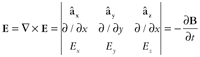
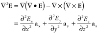
Since most of us do not work with Maxwell’s equations on a daily basis, a quick overview of the mathematical notation used in (1) through (4) will help strengthen our intuitive understanding of the physics behind undesired radiation. In the Cartesian coordinate system, the del differential operator is defined as Applying the del operator to different electromagnetic field quantities tells us how the fields behave in space. If we combine the del operator with the vector dot product and then apply it to a vector, we get the divergence, or div, of that vector. For example, applying this combination to the displacement flux density, D, results in Gauss’s law for electric fields. div From (7) we can see that Gauss’s law relates a spatial property of the electric field at a point, its divergence —•D, to a known quantity, the charge density qv, at that point. How much the electric field diverges from a point is dependent on the amount of charge located at that point. If we combine the del operator with the vector cross product and again apply it to a vector, we get the curl of that vector. Applying this combination to the electric field, we get Faraday’s law. curl From (8) we can see that Faraday’s law also relates a spatial property of the electric field at a point, the curl of the electric field —¥ E, to the time rate of change of magnetic field occurring at that point. We can use the del operator to define other spatial relationships. For example, we can define the Laplacian of the electric field, —2E, as the gradient (grad) of the divergence of E minus the curl of the curl of E.
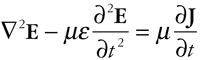
What is important to keep in mind is not the detailed mathematical manipulations required to come up with expressions such as (9), but the fact that expressions containing the del operator, —, describe some aspect of the spatial characteristics of electric and magnetic fields at a point in space. If we confine ourselves to regions of space where the materials properties, e, m, and s, are linear, isotropic, and homogenous - an assumption we can confidently apply to our case where good conductors are surrounded by air - we can take the first two relationships of (5), substitute them into (3) and (4), and after some crafty mathematical thrashing about that includes (9), we arrive at the following three elegant equations [3].
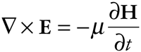
From (10) we can see that a time varying current, J, creates a distortion in the electric field, E, (e.g. an electric field that varies both in time and space) around the current carrying conductor. In the region of space around the wire, we can set the conduction current in (3) to zero, in which case (3) can be expressed as (11). Once a time varying electric field is created, then (11) says a distortion in the magnetic field is also created, which in turn creates a distortion in the electric field (12). Equation (10) is the governing equation that describes how a distortion in the electromagnetic field is launched, while (11) and (12) describe how this distortion propagates through space. If the current, J, does not vary in time, for example when there is no current flowing or the current is flowing at a constant (DC) rate, then no time varying distortions are created in the electric field, and no propagating electromagnetic field is created. Since current is defined as the velocity of charge, the derivative of the current is equal to the acceleration of charge. Equations (10) through (12) basically state that whenever we have acceleration of charge, we create propagating electromagnetic fields. An analogous process occurs in all physical waves, even the spectator “waves” so popular at sporting events. Referring to Figure 2, a “source” spectator launches a wave by standing up and then sitting back down. The spectator sitting beside the source decides to do the same, and also stands up and sits back down. The third spectator, sitting beside the second spectator, also decides to participate. The process continues on, and the “wave” starts propagating down the bleachers. Once the wave is launched, the “source” spectator is no longer needed. He/she can leave to go buy another soft drink or hot dog, and the wave will continue unimpeded. We should note that neither the electromagnetic wave or the spectator wave, travel at infinite velocity, both waves exhibit time retardation. Once the source of the electromagnetic wave, the accelerating charges that form the basis for the time varying current J, launch the wave in accordance with (10), the wave continues on its own volition in accordance with (11) and (12). The charge, no longer needed to maintain the outwardly propagating wave, can then concentrate on other things, like heating up the wire. Electric Fields Around a Positive Charge While (10) through (12) make sense from a conceptual point of view, they tell us little about what the distortion we created in the electromagnetic field looks like. To find out exactly what is happening, we can study the electric field around a collection of stationary charge, briefly accelerate the charge to a DC current level, wait for a short period of time to let the distortion propagate outward a bit into space, and then decompose the distortion into vector components tangential and normal to the direction of propagation. Figure 3 shows a cross section of a sphere surrounding the charge centered at the origin, O. Lines of electric flux emanate radially outward from the charge. The lines of electric flux only show vector direction, not magnitude. They show the path a small positive test charge would follow if we placed it in the field and then let it go. Within the engineering world, a variety of methods are used to indicate magnitude, including varying either the length or the thickness of the vector line in proportion to its magnitude. In our case the spacing between the lines of flux is used to represent the magnitude of the electric flux density, D. As we approach the charge, the lines of flux come closer together and the magnitude of the flux density, D, increases. As we move away from the charge, the lines of flux spread farther apart and the magnitude of D decreases. By taking Gauss’s law (1), integrating both sides over the entire volume of the sphere, and then applying the divergence theorem, we find the flux density, D, and electric field, E, are equal to [5].
From (13) we can see the electric field also varies with increasing/decreasing distance from the source. Restrictions on Lines of Flux There are several other subtle points we need to address with respect to lines of flux. Gauss’s law (1) states that at points where charge exists, the divergence of D is not zero. Geometrically this means lines of flux either start (if the net charge density is positive at the point of interest) or end (if the net charge density is negative). At the center, O, —·D þ 0, charge is present AND lines of flux line start from that point. Conversely, at points where —·D = 0, no charge is present AND no flux lines start from or terminate at that point. In region Vk, no charge exists, and hence field lines passing through this region must be continuous. Kinks in the Electric Field We are now ready to see what happens to the electric field when we briefly accelerate our collection of charge. Referring to Figure 4, at time t = 0, our charge is at rest at position, O, and the flux lines emanating from the charge are identical to the lines of flux shown in Figure 4. Shortly thereafter, we apply an acceleration, a, for a brief period of time, Dt, bringing the charge velocity up to v = aDt. Now the lines of flux start from point O’ instead of O. It takes a finite amount of time for the position of the new flux lines to propagate outward Ð they cannot go faster than the speed of light. On the outwardly propagating “wave-front”, for example in volume Vk, we are in a region with no charge, and Gauss’s law requires the flux lines be continuous across the wave-front. The only way this condition can hold is if the lines of flux are kinked. Since the electric flux density, D, and its associated electric field, E, are both defined in terms of the electric lines of flux, they too end up being kinked. We can therefore conclude accelerating charge creates a kink in the electric field, E. Note the kinks are not constant on the wave-front Ð they change with respect to angle. Referring to Figure 5, if we now wait for a short period of time, t, to let the kink propagate outwards a bit, the charge will have moved to the right by a distance vt = (aDt)t to point P. The field lines due to the charge must still remain connected, and so we still have a kink, although it is now a bit larger. In the limiting case, where Dt Æ 0, distance OP ª O’P ª vt = (aDt)t, and the normal component of the electric field kink, Eq, is proportional to distance AB = (aDt)t sinq. The tangential component of the kink, Er, is proportional to distance BC = cDt. Taking the ratio of these two electric field components, we get Substituting (11) for Er in (17), and noting that the distance PA = r = ct, we finally obtain the tangential and normal components of the electric field kink.
This is another good point to pause and reflect on exactly what these two equations mean from a physical standpoint. We see from (15) and (16) that the radial component of the electric field kink, Er, decreases as the square of the distance, 1/r2, while the normal component, Eq, decreases linearly with distance, 1/r. Far away from the source only the normal component of the kink remains. From (16) the magnitude of Eq is proportional to the rate of charge acceleration, a. Because current is defined as the velocity of charge, I = dq/dt, acceleration of charge occurs whenever we generate a time-varying current, dI/dt = d2q/dt2 þ 0. These results are also in agreement with (10). The magnitude of Eq is dependent sinq. From Figure 5, maximum radiation occurs at points perpendicular to the direction of charge motion, minimum magnitudes occur at points in line with charge motion. This angular dependence explains why broadside radiation from a resonant dipole antenna is maximum while end-fire radiation is minimum. And finally, we should keep in mind that (14) through (16) assumes the electron velocity, also known as the conduction drift velocity, is much less than the speed of light. For most conductors, such as copper, steel, and aluminum, this holds true. Convection electrons, inside a particle accelerator for example, can travel significantly faster, and then the relativistic forms of these expressions must be used [6]. Charge Acceleration on a Wire Segment Now let’s take a look at what happens when a digital logic device launches a pulse down a conductor towards a load. The pulse can be divided into three distinct regions. During the logical zero to one transition, region A in Figure 6, current increases, and charge accelerates. During the logical high level, region B, a constant current is flowing, and no charge acceleration takes place. And finally, during the logical one to zero transition, region C, charge deaccelerates. Referring to Figure 7, we can see during the leading and trailing edges of the digital pulse (regions A and C), the spacing between the lines of electric flux change. The electric flux density, D, and its associated electric field, E, both change with time, creating a kink in the electric field. During the logical high level, however, the spacing between the electric lines of flux remain constant, no kinks are created in the electric field. Figure 8 shows three frames from an FDTD simulation where a source launches a current pulse into a horizontal wire. The simulation supports this geometrical interpretation. Notice that as the pulse propagates down the wire towards the right, the two kinks, one due to the leading edge of the pulse, region A, the other due to the trailing edge of the pulse, region C, propagate radially outward from the location of the source. If we look closely at Figure 7, we also see the magnetic flux density changing during the logical transitions (e.g. the magnetic lines of flux come closer together during the leading edge of our pulse, and moving farther apart during the trailing edge). This does not surprise us since we know from (11) and (12) that propagating fields contain coupled electric and magnetic field components. Bends in Conductors We also need to ask ourselves what happens when the leading or trailing edge of our propagating digital pulse encounters a bend in the conductor. Referring to Figure 9, the leading edge of our digital pulse propagates down the wire with velocity, v. At time ta, the velocity is va, and a bit later, at time tb, the velocity is vb. The magnitude of the velocity, v, remains the same, just the direction changes. The acceleration, a, is defined as the time rate of change of velocity
From geometry, we can see that
\ Substituting (17) into (18) and taking the limit we get
From (19) we can see that another region where charge can accelerate is around conductor bends. A smaller bend radius increases the acceleration of charge, and produces a correspondingly larger kink in the electromagnetic field. To reduce radiation from printed circuit boards, trace right angle bends can replaced by two 45 degree bends or bends with a smooth continuous radius. Figure 10 shows an example of how this is accomplished as traces are routed through a connector via field. Figure 11 shows a serpentined delay line with rounded ends to minimize radiation from the bends. Impedance Mismatches We know from transmission line theory that terminating a transmission line into an impedance not equal to its characteristic impedance produces a reflection. As a result, a portion of the charge associated with the pulse must de-accelerate until they come to a complete stop, turn around, and then accelerate back towards the source. Impedance mismatches are also locations where charge acceleration can take place. No wonder the ends of the dipole radiate so efficiently. Figures 12 shows a cross section of a printed circuit board card edge connector from an FDTD simulation. The printed circuit board is located in the lower right corner of Figure 13. On the left are the shielded twisted pair cables. In the center are the mated sections of the two connector halves. Figure 13 graphically shows the results of the FDTD simulation when a single digital pulse propagates through the connector. As can be seen from Figure 13, a significant number of kinks propagate outward from each bend in the connector structure. Summary of Potential EMC Problem Areas Whenever charge accelerates, time/spatially varying kinks are created in the electric field surrounding the region where the charge is being accelerated in accordance with (10).
The kink in the electric field produces a propagating electromagnetic field in accordance with the coupled curl equations
Locations where charge acceleration is enhances include sources, bends with small radius of curvature, and locations in transmission line structures where a constant impedance is not maintained. References
Author Biographies Franz Gisin is Manager of EMC and Signal Integrity Design at Sanmina-SCI. He has been active in the EMC field for over 25 years, and has published numerous articles in trade journals and EMC Symposia. His current research interests focus on EMC and signal integrity issues associated with high speed PCB interconnects. He has served as a Secretary, Treasurer, Vice Chair, and Chair of the Santa Clara Valley Chapter of the IEEE EMC Society. He is a past IEEE EMC Society Distinguished Lecturer, and past member of the IEEE EMC Society Board of Directors. Currently he is vice-chair of TC-10, Signal Integrity, and Steering Committee Chair of the 2004 IEEE International EMC Symposium, Santa Clara, CA. He received his BS(EE) from the University of Idaho in 1972, and his MS(Applied Math) from Santa Clara University in 1986. Dr. Zorica Pantic-Tanner is Founding Dean of the College of Engineering at the University of Texas at San Antonio (UTSA). Prior to joining UTSA she was Director of the school of Engineering at San Francisco State University (SFSU). Pantic-Tanner’s research and teaching interests are in the areas of Electromagnetic Field Theory, Applied Electromagnetics and Electromagnetic Compatibility (EMC). She has published more than 80 papers in refereed journals and conference proceedings. Dr. Pantic-Tanner received her B.S., M.S., and Ph.D. degrees in Electrical Engineering from the University of Nish in Yugoslavia in 1975, 1978, and 1982, respectively. In 1984 she was awarded a Fulbright Scholarship for postdoctoral research in the area of Applied Electromagnetics at the Electromagnetics & Communications Lab of the University of Illinois at Urbana. Dr. Pantic-Tanner is a Senior Member of the IEEE, a member of the IEEE EMC Board of Directors, International EMC Education Committee, University EMC Grant Committee, Vice-Chair of the IEEE International EMC Numerical Modeling Committee, and Technical Program Chair for the 2004 IEEE International Symposium on EMC. She also belongs to the IEEE Women in Engineering Association, IEEE EMB Society, ASEE, SWE, and AHEE. |
 (8)
(8)
 (9)
(9)
 (10)
(10)
 (12)
(12)|
If you would
like to contact the IEEE Webmaster |