|
 |
|
|

Technical
Seminar |
|
|
|
|
|
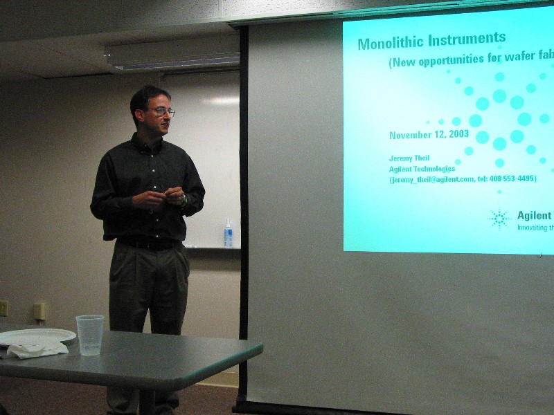
Monolithic Instruments -- New Opportunities for
Wafer Fabs
|
|
|
DATE/TIME
Wednesday, November 12, 2003
(4:30pm to 6:00pm)
|
|
PLACE
Engineering
Bldg. B101 (first floor) (CSU,
Fort Collins, CO)
|
|
|
ABSTRACT As CMOS process technology has matured over
the past few years, a novel trend is emerging in which new materials
and structures are being integrated into or onto the integrated
circuit (IC) to create novel devices. Monolithic instruments are
systems or sub-systems that combine conventional IC's with novel
solid-state sensors/actuators so that they can interact with their
physical environment. Such systems can achieve cost and
performance enhancements through integration and
miniaturization. Examples include a-Si:H photodiode arrays, OLED-based
microdisplays, integrated biological and chemical detection systems,
integrated optical and photonic systems, and digital micromirror
displays. A non-exhaustive list of materials include those that
can be incorporated into IC's such as (i) deposited semiconductors
such as a-Si:H and microcrystalline silicon, (ii) OLED (organic LED)
materials; (iii) polycrystalline Si, (iv) chemically active and inert
conductors; (v) organic conductors; (vi) biocompatible materials; and
(vii) magnetic thin films. This presentation briefly touches on
various types of monolithic devices that have been fabricated, and
concentrate on issues pertaining to a-Si:H and OLED-based arrays to
highlight the advantages of such devices as well as the challenges
they present in design and manufacturing. |
|
PRESENTATION SLIDES
pdf |
|
|
DR. JEREMY A. THEIL
(Agilent Technologies, Santa Clara, CA)
|
|
|
Jeremy Theil is a Principal
Project Scientist at Agilent Technologies, Santa Clara, CA, working on
advanced process technologies for mixed signal processes, and novel
solid-state devices. He has been with Agilent for eight years,
spending the first four years at HP Labs working on CMOS BEOL process
development. While there, he developed a state-of-the-art a-Si:H
photodiode array technology for advanced CMOS imager applications. He
also has experience in low-K dielectric material and process
development, optoelectronic test development, device design and
simulation, and 1/f noise measurements. Prior to joining
Hewlett-Packard, he worked at Johnson Controls developing thin film
gas diffusion barriers. He received his PhD in Materials
Science and Engineering from North Carolina State University, Raleigh,
NC, and is author on 28 papers and 33 patents. He recently served on
the editorial board of the Journal of Vacuum Science and Technology. |
|