|
 |
|
|
Technical
Seminar Distinguished
Lecturer Series |
|
|
|
|
|
Negative Bias Temperature Instability (NBTI):
Physics, Materials, Process and Circuit Issues
|
|
|
DATE/TIME
Thursday, August 11, 2005 (4:30-6:00pm) |
|
PLACE
Bldg. 1 Auditorium (Agilent Technologies,
Fort Collins, CO) |
|
DIRECTIONS
From I-25, take Harmony Road Exit (Exit
265) westbound, and enter Agilent/HP campus on right. Agilent/HP
campus is on the NE corner of Harmony Road and Ziegler Road.
Proceed to Bldg. 1 Lobby to sign-in and meet host for escort to
Auditorium. |
|
Non-Agilent/HP/Intel
Attendees: Please arrive punctually at 4:15pm as you will need to be
escorted to the seminar room. We appreciate a courtesy RSVP to
bob_barnes@agilent.com to
expedite sign-in and to help us with a headcount estimate for
food/drinks. |
|
|
ABSTRACT
|
|
In this talk I will
present an overview of negative bias temperature instability (NBTI)
commonly observed in p-channel MOSFETs when stressed with negative
gate voltages at elevated temperatures. The talk will
concentrate on the physics, materials, process, and some circuit
issues, e.g., dc versus ac stress. I discuss the results of
such stress on device performance and review interface traps and
oxide charges, their origin, and present understanding of NBTI.
Next I discuss the effects of varying parameters (hydrogen,
nitrogen, water, fluorine, deuterium, boron, temperature, electric
field, and gate length) on NBTI and conclude with NBTI and
minimization. |
|
PRESENTATION SLIDES
pdf
|
|
|
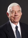
PROF. DIETER
K. SCHRODER (Arizona
State University, Tempe, AZ)
|
|
Dieter K. Schroder
has worked with semiconductor material and device
electrical characterization for the last 35 years. He
received his
education at McGill University, Montreal, Canada, and at the University
of Illinois, Urbana-Champaign, IL. He joined the Westinghouse
Research Labs in 1968 where he was engaged in research on various
aspects of semiconductor devices, including MOS devices, imaging arrays,
power devices, and magnetostatic waves. He spent a year at the
Institute of Applied Solid State Physics in Germany during 1978.
In 1981, he joined Arizona State University in the Center for Solid
State Electronics Research. His current interests are
semiconductor devices, defects in semiconductors, semiconductor material
and device characterization, low power electronics, and device modeling.
He
has written two books Advanced MOS Devices and Semiconductor
Material and Device Characterization, has published over 150 papers,
has graduated 91 graduate students, has given many short courses and
is a Life Fellow of IEEE. |
|
Website |
|
|
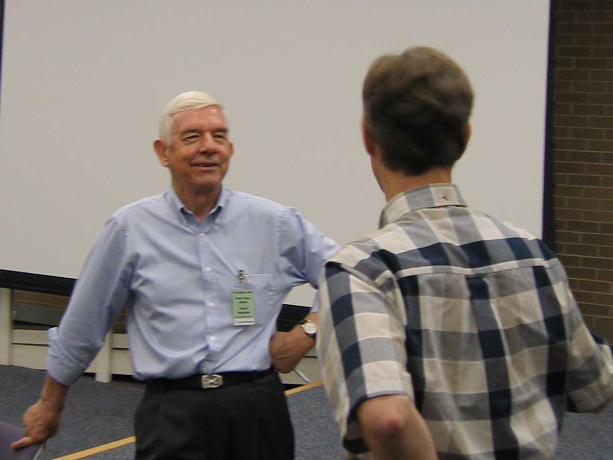
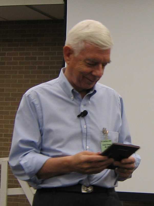
PHOTOS
Courtesy of Bob Barnes
|
|
 |
|
 |
|