|
 |
 |
|

Technical
Seminar |
 |
 |
|
|
|
Analog Design in Sub-100nm Technologies |
|
|
DATE/TIME
Thursday, June 29, 2006 (4:30pm to 6:00pm) |
|
PLACE
Bldg. 1 Auditorium (Avago
Technologies, Fort Collins, CO, formerly Agilent Technologies) |
|
DIRECTIONS
|
|
Non-Avago Attendees:
Please arrive punctually at 4:15am as you will need to be escorted to
the seminar room. RSVP to
bob.barnes@avagotech.com
to expedite sign-in and to help us with a headcount estimate for
food/drinks. |
|
From I-25, take Harmony Road Exit (Exit 265) westbound, and enter
Agilent/HP campus on right. Avago/HP/Intel campus is on the NE
corner of Harmony Road and Ziegler Road. Proceed to Bldg. 1 Lobby
to sign-in and meet host for escort to Auditorium. |
|
COST
Free. As always, food &
drinks will be provided. |
|
|
ABSTRACT
|
|
For the past 10-20 years, the
analog/mixed-signal design community has been debating the "negative"
impact of feature size scaling on analog design. While reduced
supply voltages, low device gain, and leakage currents are certainly of
concern, these factors only conditionally deteriorate performance.
In many cases, the associated shortcomings can be overcome using
appropriate design strategies and architectural adjustments. |
|
In this talk, we'll take a more
optimistic look at the future of analog circuitry in sub-100nm CMOS
technologies. Followed by a survey of device parameters and their
impact on analog design, we'll highlight a number of architectural
opportunities that may help sustain the current trend of ever-improving
performance and power dissipation. |
|
PRESENTATION SLIDES
pdf |
|
REFERENCES
links to publications |
|
|
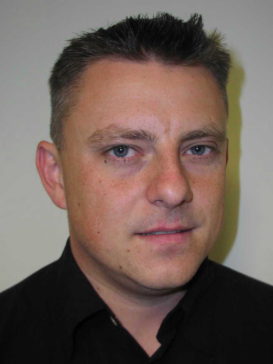
PROF. BORIS
MURMANN (Stanford University, Stanford, CA)
|
 |
Boris Murmann
received the Dipl.-Ing. degree in Communications Engineering from FH
Dieburg, Germany in 1994. He received the MS degree (with
distinction) in Electrical Engineering from Santa Clara University in
1999. In 2003, he received the PhD degree in Electrical
Engineering at the University of California, Berkeley, with a
dissertation focusing on high performance A/D conversion.
From 1994 until 1997 he was with Neutron Mikrolektronik GmbH, Hanau,
Germany, where he was involved in the design of high-voltage,
smart-power, and low power ASICs in CMOS technology. In 1992 and
1999, he held Engineering Intern positions in the field of Analog
Circuit Design with R&E International Inc., King of Prussia, PA.
During the summer of 2001, Dr. Murmann was with the High-Speed Converter
group of Analog Devices, Wilmington, MA. Since 2004, he is with
the Department of Electrical Engineering at Stanford University, where
he serves as an Assistant Professor.
|
|
In the year 2000, Boris
Murmann received the EECS Outstanding Graduate Student Instructor award
from UC Berkeley. In 2001, he was a recipient of the Analog
Devices Inc. Outstanding Student Designer award. In 2003, Dr.
Murmann received the
CalVIEW Citris Award for
Excellence in Distance Education. |
|
Website |
|
|
|