2010 Meetings
The linked titles of some meetings are the presentations speakers provided.
December 14, 2010: Joint meeting with SCV-PSES chapter " EMC/EMI Issues in Biomedical Research" by Prof. Ji Chen, ECE Dept., University of Houstonn
Abstract: The interactions between electromagnetic signals and biomedical systems lead to safety considerations for medical devices and patients. In this talk, we will present some recent investigations on the EMC/EMI issues related to these scenarios. In particular, we will discuss 1) safety evaluation for pregnant woman under walk-through metal detector, 2) thermal and temperature evaluation of pregnant woman models under MRI RF coil, 3) effects of implantable devices within human subject models under MRI coils, and 4) the interactions between vehicular mounted antenna and bystanders with implantable medical devices.

Bio: Dr. Ji Chen received the Bachelor's degree from Huazhong University of Science and Technology, Wuhan, Hubei, China, the Master's degree from McMaster University, Hamilton, ON, Canada, in 1994, and the Ph.D. degree from the University of Illinois at Urbana-Champaign in 1998, all in electrical engineering. He is currently an Associate Professor with the Department of Electrical and Computer Engineering, University of Houston, Houston, TX. Prior to joining the University of Houston, from 1998 to 2001, he was a Staff Engineer with Motorola Personal Communication Research Laboratories, Chicago, IL. Dr. Chen has received outstanding teaching award and outstanding junior faculty research award from College of Engineering at University of Houston. He is also the recipient of ORISE fellowship in 2007. His research group also received the best student paper award at IEEE EMC Symposium 2005 and the best paper award from IEEE APMC conference in 2008.
November 9, 2010: "War Stories from EMCS Founders" by Jerry Ramie
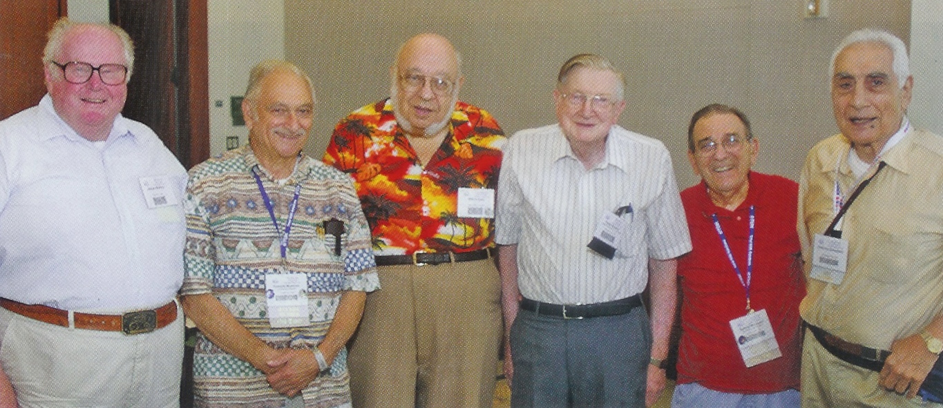
Abstract: Six of the original founders of the EMC Society were invited to the 50th Anniversary celebration of the formation of the EMC Society in Honolulu, HI in July of 2007. Tony Zimballati, Dr. Ralph Showers, Jim McNaul, Vince Mancino, Milton Kant and Sam Burrauno spoke in the EMC History theatre and told riveting stories of the early years of the EMC profession. The host is Dan Hoolihan, our EMC Society historian.
The video of this event is posted at the IEEE global history network. It lets six of the founding members of the EMC Society tell the "war stories" that they thought were important in their careers. It's funny, serious, touching and always true to life, including many photos of the people, places and things that are discussed. 72 minutes. (produced by Jerry Ramie)
October 12, 2010: "Spacecraft and Surface Charging Mitigation" by Dr. Richard Briët, Aerospace Corporation
Abstract: Dr. Briët will talk about Spacecraft and Surface charging with emphasis on practical applications of the current State of the Art of Spacecraft Charging Mitigation. For tonight's Blue Light Specials, Dr. Briët will briefly discuss new developments in the use of Surface Charging as an enabling process to detect Subsurface Defects, and to use Reverse Engineering of Current Transients from electrostatic discharges as a means to locate the initiation points of ESD on solar panels.
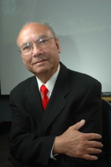
Bio: Dr. Briët earned his doctorate degree in Solid State Physics (Nuclear Magnetic Resonance and Plasma Physics) and Mathematics at the University of Utah in Salt Lake City, UT.
After an exciting and challenging career in Survivability, Vulnerability, and Endurability at Boeing, Military Aircraft Company in Wichita, KS, General Dynamics, Convair Division in San Diego, CA, and TRW, Redondo Beach, CA, Dr. Briët joined The Aerospace Corporation, an FFRDC (Federally Funded Research and Development Center) in El Segundo, CA, where he was assigned additional responsibilities in support of many Commercial and Non-Commercial Space Programs.
Through his many publications and presentations at National and International Conferences in the US of A, France, Germany, The Netherlands, the United Kingdom, Taiwan, and Japan, Dr. Briët has become a widely recognized expert in Plasma Physics, Electromagnetic Effects, Lightning, and Space Radiation Effects.
September 23 - 24, 2010: SCV-EMC 2010 Mini Symposium
Abstract:
September 23: "EMC Modeling and Design" by
Dr. Todd Hubing, Michelin Professor of Vehicle Electronics, Clemson University
Morning Session: 8:00 AM - 12:00 PM
- Power Inverter / Motor Design for Reduced Emissions
- Grounding and Shielding in Mixed Signal PCBs
Afternoon Session: 1:30 PM - 5:00 PM
- Component Characterization for System-Level Modeling
- How Productive EMC Engineers use Computer Modeling Tools
Morning Session: 8:00 AM - 12:00 PM
- Part I: Radiated Immunity
- Part II : Co-site Interference
Bios:
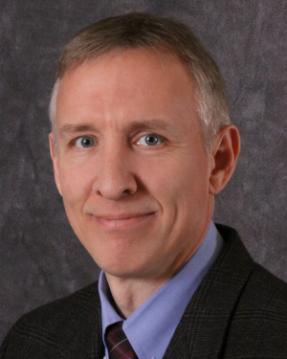 Dr. Todd Hubing is the Michelin Professor of Vehicle Electronics at Clemson University. He
holds a BSEE from MIT, an MSEE from Purdue, and a Ph.D. from North Carolina State University. He began his career
as an EMC engineer for IBM in 1982, where he did EMC testing and troubleshooting on a variety of computer and
network communications products. In 1989, he became a faculty member at the University of Missouri-Rolla (UMR)
where he worked with other faculty and students to analyze and develop solutions for a wide range of EMC problems
affecting the electronics industry. Since moving to Clemson in 2006, he has continued his work in electromagnetic
compatibility and computational electromagnetic modeling, particularly as it is applied to automotive and
aerospace electronics. Dr. Hubing is a Fellow of the Institute of Electrical and Electronics Engineers (IEEE) and
a Fellow of the Applied Computational Electromagnetics Society.
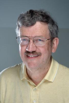 Dr. Tom Jerse has over 30 years experience with Hewlett-Packard and Boeing in solving EMI
problems both at the circuit and systems level, and has earned a PhD in EMC from the University of Kentucky. He
presently holds the dual positions of Professor of Electrical Engineering at The Citadel and Associate Technical
Fellow of the Boeing Company. He served two years as a distinguished lecturer of the EMC Society, and has
developed and taught original EMC courses at the professional and university level since 1981.
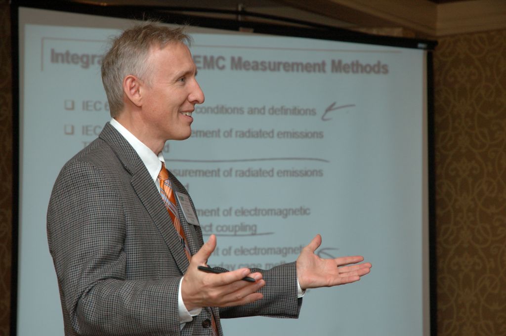
The above clickable picture slideshow illustrates some of the event and some of the lucky raffle winners (not all
vendors/winners are featured)
June 9, 2010: joint meeting with SCV-CPMT "Novel Fine Pitch, Low Profile, Low Cost Connector Technology" by David Light, VP Technology, Neoconix, Inc.
Abstract: This talk will present a revolutionary connector technology providing unparalleled design flexibility at low cost. A photolithographic approach to connector definition coupled with batch, printed circuit manufacturing methods allows highly configurable designs. Pin-out modifications, electrical performance tuning, tailoring of mechanical characteristics, and even adjustment of connector thickness can be accomplished quickly and easily with CAD modifications to low cost photo-masks and/or by modifications to the bill of materials. Connectors can be custom designed and fully optimized for each revision or generation of a product, with minimal tooling costs and lead time. Lithographically defined contact arrays also enable high levels of integration and miniaturization - pitch is no longer limited by the practical limitations of injection molding connector housings into which free standing spring contacts are subsequently stitched. Neoconix utilizes a MEMS process model, implemented using the low-cost printed circuit substrate infrastructure, to fabricate contact arrays that can scale with advances in photo-lithography and HDI printed circuit substrate technology.
The connector fabrication process starts by defining arrays of copper alloy beams, in sheet format, in their ultimate configuration using large format, batch lithography and etch methods. The arrays of beams, still in sheet format, are then formed into three dimensional, 'S'-shaped cantilever beams, using low cost, programmable dies. The sheets of contact arrays are subsequently integrated into connector 'interposer' structures using standard printed circuit fabrication processes, including lamination, plating, and etching. The resulting one or two sided contact arrays can function as freestanding interposers or are readily integrated into standardized, low cost connector housings that provide alignment, attachment and actuation.
This talk will review basic elements of the Neoconix PCBeam technology, and will use real-world applications as well as simulations to describe recent learning on the relative impact of the flexible design elements on signal integrity and bandwidth, mechanical characteristics, durability, contact resistance, and reliability, and will describe applications where system level designs have been improved from a functional, form factor and/or cost perspective by implementing Neoconix interconnect structures.
Bio: David Light is Vice President, Technology at Neoconix, Inc. Prior to joining Neoconix in September, 2009, he was an independent consultant in providing ongoing and project-based services in technology development, intellectual property evaluation, business strategy, and technology marketing to clients including Tessera, Samtec, Flint Hills Solutions, Microconnex, Coleman Research Group, Latham and Watkins, and Neoconix, in areas spanning microelectronics packaging, high density substrates, and surface mount technology. His career has included fundamental process and materials R&D, process and product development, technology management, marketing and business development, manufacturing operations, and General Management. His areas of expertise include substrates and printed circuits, semiconductor packages (including assembly, test and burn-in), interconnect technologies, test tooling, and miniaturized electronic systems. David's career began at the IBM T.J. Watson Research Center, in the electrochemical studies group, and has included technology and business leadership positions at IBM Microelectronics, Tessera, Flex2Chip, and Sunright/KES Systems.
David is a graduate of Stanford University. He has over three dozen issued US patents and has authored numerous technical publications and presentations. He is a member of IEEE CPMT.
May 11, 2010: "How to Apply Shielded Cables to Solve More Problems than You Create" by Dr. Tom Jerse
Abstract: Shielded cables are widely used to enhance signal integrity and solve interference problems, but there are several mechanisms that if not understood in a system design can inadvertently cause interconnect cables to become the dominant player in crosstalk or radiated emissions. This talk explains the ways in which cables can both mitigate and exacerbate electromagnetic interference, and presents basic design principles and troubleshooting techniques for achieving the most electromagnetically compatible designs possible.
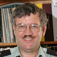
Bio: Tom Jerse has over 30 years experience with Hewlett-Packard and Boeing in solving EMI problems both at the circuit and systems level, and has earned a PhD in EMC from the University of Kentucky. He presently holds the dual positions of Professor of Electrical Engineering at The Citadel and Associate Technical Fellow of the Boeing Company. He served two years as a distinguished lecturer of the EMC Society, and has developed and taught original EMC courses at the professional and university level since 1981.
April 13, 2010: "1) Demystifying Radio Frequency Fields and Radio Frequency Components" &"2) Aiding the 17025 Laboratory Accreditation Process by Capturing Key Performance Data on RF Power Amplifiers" by Tom Mullineaux, MILMEGA Limited
Abstract: 1) This presentation looks at situation the great 18th and 19th century masters faced along the uncharted road from static electricity to the prediction and discovery of RF fields. The story picks up with Benjamin Franklin's contribution to static electricity and then describes the 'great race' that followed the accidental discovery that an electric current deflects a compass needle. The talk is rounded off with an explanation of the working of common RF components.
2) RF immunity standards do not require periodic calibration of the RF amplifiers used in RF immunity testing. This is justified from a strictly technical point of view, yet creates the situation where there is no data on file for the most expensive piece of equipment in the test set-up. This presentation goes through the key amplifier performance metrics, and introduces a simple/swift method of capturing key data that can be held on file as 'trend-analysis' data.
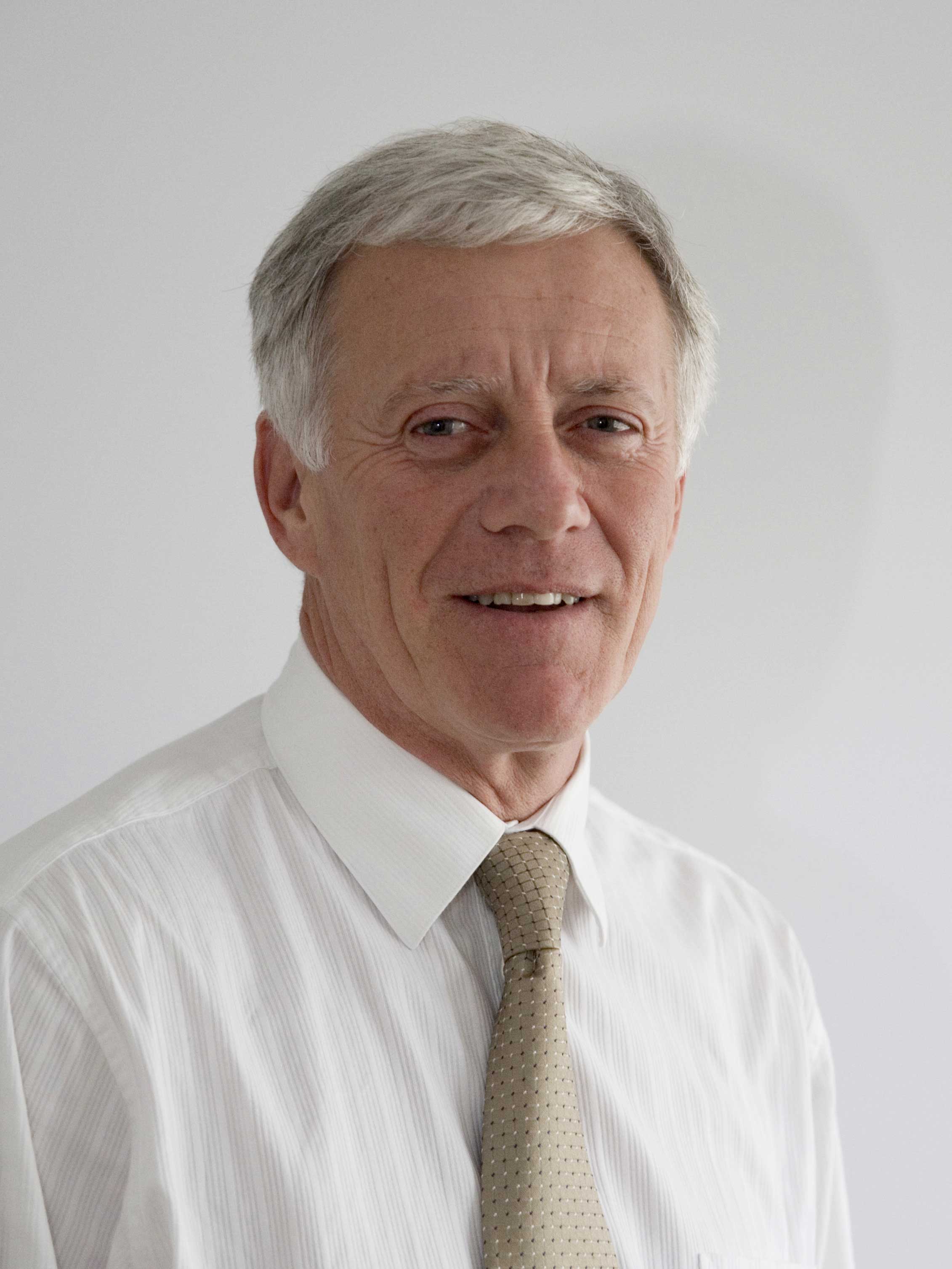
Bio: Tom is an RF engineer with experience in leading RF design teams in the design and development of high-power microwave amplifiers for use in defense and commercial applications. Tom received his degree in electrical and electronic engineering from Portsmouth University, England in 1989. He has delivered both practical and theoretical presentations to IEEE EMC Society sponsored events including 'Linearization of an RF Amplifier for Immunity Testing' at the 2004 Santa Clara EMC Symposium, and has had many technical articles published, including 'Rating Power Amplifiers for RF Immunity Testing' for Evaluation Engineering Magazine , 2003; 'Selecting antenna/power amplifier combinations for the coming new RF immunity standards' for Interference Technology Magazine 2004; 'Using radar amplifiers for automotive RF immunity tests' for Evaluation Engineering Magazine, 2005.
March 9, 2010: "An Overview of Chip Level EMC Problems" by Dr. Sergiu Radu, Sun Microsystems
Abstract: The CPUs and the VLSI chips are the primary sources of electromagnetic noise in all electronic equipments. Reducing the electromagnetic noise at source level is usually the best and the most economical solution. The presentation discusses typical interference mechanisms associated with CPU/VLSI, as well as mitigation methods at die-level and package level. Among the aspects discussed are some power distribution issues, on-die decoupling, package capacitors, routing aspects, the impact of back-bias and forward-bias, and the impact of die-shrinks on the EMI performance of the VLSI chips.
Outline:
- Introduction. EMI mechanisms for VLSI chips
- Heatsink effect for large VLSI chips
- Back-bias impact on EMI
- Integrated and separated power distribution
- Noise injection into the PCB
- Package level improvements for EMI
- Die level improvements for EMI
- Second harmonic emissions
- Power distribution issues
- Spread Spectrum Clock Generation
- Die-shrink impact on EMI
- Conclusions
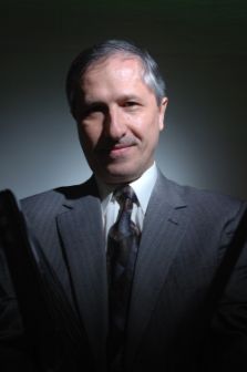
Bio: Dr. Sergiu Radu is currently Principal Engineer at Sun Microsystems, leading the EMC Design group in Menlo Park, California. His role at Sun includes the development and implementation of architectural frameworks for EMC Design through design guidelines and best practices, and to provide forward looking solutions, root cause analysis of significant EMC problems, design methodologies involving software simulations and better prediction techniques. Sergiu Radu received a M.S. and a Ph.D. in Electrical Engineering (Electronics) from Technical University of Iasi, Romania, and until 1996 he was an Associate Professor at the same university, involved in Electromagnetic Compatibility teaching and research. From 1996 until 1998 he was a Visiting Scholar, as part of the Electromagnetic Compatibility Laboratory, at the University of Missouri-Rolla, currently Missouri University of Science and Technology. In 1998 he joined the EMC Engineering group at Sun Microsystems. Sergiu holds seven US patents for EMI reduction techniques in electronic systems and has many papers published in research journals, symposia, and magazines. He is a reviewer for IEEE Transactions on EMC. He is also a 2009-2010 Distinguished Lecturer for the IEEE EMC Society.
February 9, 2010: "Common Misconceptions about Inductance and Current Return Path" by Dr. Cheung-Wei Lam, Apple
Abstract: In today's high-speed digital system design, a good understanding of inductance and current return path is important to signal integrity and EMI control. Unfortunately, several key concepts about the two have often been misunderstood or overlooked. This presentation will discuss the key concepts and some common misconceptions about inductance and current return path. Examples will be given at the chip and PCB levels.
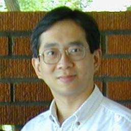
Bio: Dr. Cheung-Wei Lam is currently the Chief EMC Technologist at Apple, where he has implemented a fully automated and customized EMC layout and schematic checking system. At Apple, he is also engaged in chip, PCB and system level EMC design and research. Prior to joining Apple, he was a Co-Founder and Principal Engineer at Transcendent Design Technology and, earlier, a Principal Engineer in Viewlogic's Advanced Development Group (formerly Quad Design Technology). From 1988 to 1993, he was with the MIT Research Laboratory of Electronics, where his focus was on modeling of high-speed interconnects and superconducting transmission lines.
Dr. Lam received the B.S. degree in electronics from the Chinese University of Hong Kong, and the S.M. and PhD degrees in electrical engineering and computer science from MIT. He has authored or presented numerous technical papers and presentations on EMC and signal integrity related subjects in the US, in Europe and in Asia. He was a co-recipient of the best paper award at the 1996 IEEE EMC Symposium. He is a past IEEE EMC Society Distinguished Lecturer and currently serves in the IEEE EMC Society Respected Speakers Bureau. He has also served on the IEEE EMC Society TC-9 Computational Electromagnetics committee, the IEEE EMC Society TC-10 Signal Integrity committee, and the SAE EMC Modeling Task Force committee.
January 12, 2010: "Ultra-Thin Embedded Capacitance Laminates and how they improve the PDN and can Impact EMC" by Bob Carter, Oak-Mitsui Technologies
Abstract:
- Typical/ Traditional PDN
- The PDN using embedded capacitance
- Some Causes of Resonance and EMC in PCB's
- Ultra-Thin Laminates for Embedded Capacitance and the reducing impact on EMC
- Some practical results / case studies
- What's Next
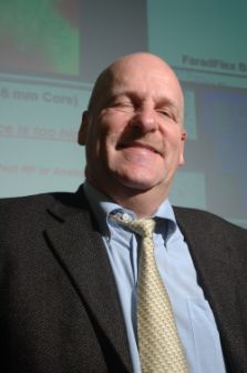
Bio: Bob Carter obtained a BS Degree in Chemical & Materials Engineering and Business Management at California Polytechnic University, Pomona, California and Grand Canyon University, Phoenix, Arizona. He has over 27 years professional experience in the printed circuit, advanced electronic materials, and chip packaging industries. He spent extensive time supporting engineering, marketing, and sales, worldwide. He initiated the start-up of 2 PCB factories in Shenzhen and Suzhou, China. He led design, engineering, development, and applications organizations at companies such as Xerox, Toppan, Multi-Fineline Electronix (M-Flex), Rogers Corporation, Flex2Chip Inc. (Tessera), Matsushita/ Panasonic Electronic Materials, and Oak-Mitsui Technologies. Currently Bob is a Senior Technology Executive supporting Oak-Mitsui and FaradFlex Embedded Capacitance materials. He is actively involved in technology leadership committees in the IPC, IEC, and IEEE.