by W. Scott Bennett
A simple, straightforward approach is described for minimizing the fields of any electrical circuit. The method is based on a study of the causes of the fields — circuit currents, and circuit geometries — rather than a study of the fields themselves.
The current element is a differential length of current that is assumed to be isolated in free space. Now, because of its assumed isolation, the current element is a concept; it is not something that can be physically realized. However, the current element is a very useful concept, because any circuit current can be accurately modelled as a superposition of its current elements. And, the electromagnetic fields of any circuit current will be equal to the superposition of the electromagnetic fields that each of its current elements would have [1-4]. Therefore, since unexpected electromagnetic fields of circuit currents are the sources of EMI, the current element is the basic source of EMI. And, the minimization of the fields of all current elements is obviously the key to EMC.
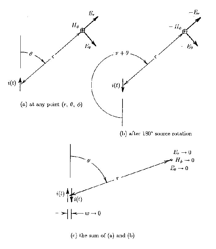
Figure 1. Current element fields.
Now, as shown in Fig. 1(a) and (b), equal current elements with opposite directions would have equal, oppositely directed, electromagnetic fields at every corresponding point in space. This follows, because each field component of an upwardly positive current element is directly proportional either to sin q, or to cos q [1-4]; and, if that current element is rotated 180ỳ, those proportionalities become sin (q +p)= –sinq, and cos (q +p) = –cosq. As a result, if two equal, oppositely-directed current elements were placed closely parallel to one another, the sums of their fields would approach zero, as shown in Fig. 1(c). Therefore, if the oppositely-directed equal of every current element can be found in a circuit, and if all such equals can be positioned closely parallel to one another, the fields of that circuit current will approach zero.
In other words, EMC can be achieved by taking two steps: (1) be sure that every current element of a circuit has an oppositely-directed equal, and (2) place the current elements of each pair of oppositely-directed equals as close and as parallel to each other as possible.
Now, an electric current is the flow of electric charge. For example, the charge flow that is the current in a metal conductor is the flow of electrons. Therefore, when the conduction current from a time-varying source increases, more electrons start to flow out of one source terminal and more electrons start to flow into the other source terminal. And, when that conduction current decreases at the source, fewer electrons start to flow out of one source terminal and fewer electrons start to flow into the other one. Also, in both cases, those changes in electron flow propagate away from the source and toward the load. In other words, one current component leaving the source propagates in the direction of positive current, and the other current component propagates in the opposite direction — one clockwise, and one counterclockwise. As a result, when they come together, at any point in the circuit, both current components have the same positive direction and their sum is the total current at that point.
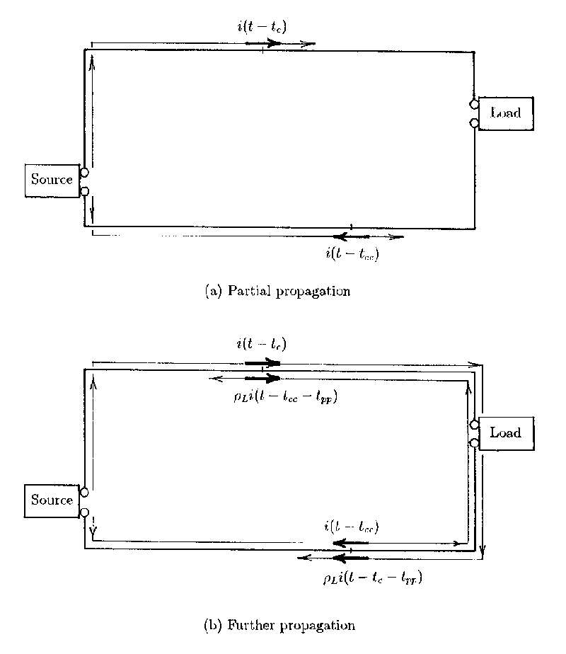
Figure 2. Circuit current components.
These current characteristics are illustrated in Fig. 2. In Fig. 2(a), i(t – tc) is the clockwise propagating current component at the upper point shown, where tc is its propagation time from the upper source terminal to that point. And, i(t – tcc) is the counterclockwise propagating current component at the lower point shown, where tcc is its propagation time from the lower source terminal to that point. In these expressions,
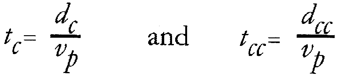
where vp is propagation velocity, dc is the distance from the upper source terminal to the upper point, and dcc is the distance from the lower source terminal to the lower point. After the additional propagation time, tpp, from point to point, the total current at the upper point will be the sum of i(t – tc) and rLi(t – tcc – tpp). And, at the lower point, the sum of i(t – tcc) and rLi(t – tc – tpp) will be the total current. This is illustrated in Fig. 2(b). In these expressions, rL accounts for the effect the load has on the amplitude of currents passing through it as a result of i2R losses, and tpp includes any time change induced by the load as the result of capacitance or inductance. The effect of the load on current components propagating in either direction is the same, because the current components have the same positive direction as they pass through the load.
Thus, if the points in Fig. 2 are equidistant from the source, then dc = dcc and tc = tcc , and the total currents at those points will be equal. However, the total current in one conductor is positive in the direction from source to load, and the total current in the other conductor is positive in the direction from load to source. Therefore, if the conductors from a circuit’s source terminals to its load terminals are given exactly the same length, every current element in one conductor will have an oppositely-directed equal in the other. And, the first step toward obtaining EMC for that circuit will have been taken.
As observed above, if both source-to-load conductors of a circuit have the same length, then every current element in that circuit will have an oppositely-directed equal. Therefore, to achieve EMC, all that remains to be done is to make the two members of each of those oppositely-directed current element pairs parallel and as close to one another as possible. A geometry that meets those requirements is illustrated in Fig. 3. As shown in that figure, the pairs need not form a straight line. However, by reducing the distance from source to load, the circuit’s fields would be further reduced, because the total number of current element pairs would be lessened.
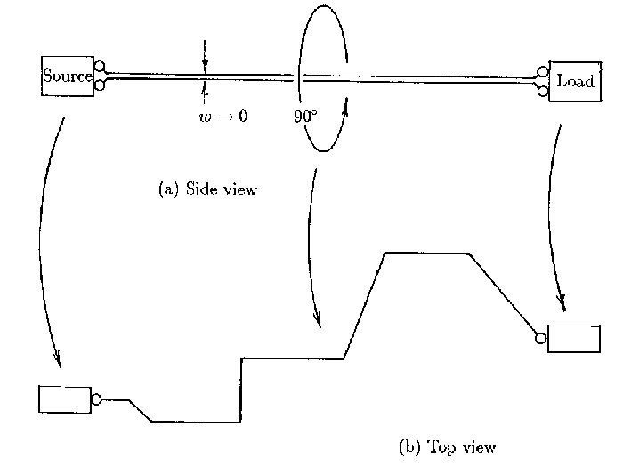
Figure 3. Typical circuit geometry for EMC.
It should be noted that an alternate method of implementation to that of two individual conductors can be obtained with one conductor close to a ground plane. However, two things should be kept in mind if a ground plane is used: (1) the spacing between a current element and its oppositely-directed image in the ground plane is effectively twice the distance between the current element and the ground plane, and (2) there will be no fields on the opposite side of the ground plane from the current element with an ideal implementation. In other words, for a given spacing between two conductors, or between one conductor and a ground plane, there will be quite different results. On one side of the ground plane there will be considerably less field cancellation than that of a conductor pair with the same spacing, and on the other side of the ground plane there will generally be near-complete cancellation. However, for a given spacing, two individual conductors will, in general, be more effective than one conductor and a ground plane.
Finally, it should also be noted that complete cancellation of the fields of oppositely-directed, equal current elements is obtainable by making them coaxial. In other words, for the ultimate in EMC, a circuit’s source-to-load conductor pair should be coaxial.
1. Hayt, Engineering Electromagnetics, McGraw-Hill, 1981, pp. 479-482.
2. Jordan and Balmain, Electromagnetic Waves and Radiating Systems, Prentice-Hall, 1968, pp. 642-644.
3. Ramo, Whinnery, and Van Duzer, Fields and Waves in Communication Electronics, John Wiley & Sons,1965, pp. 317-323.
4. Adler, Chu, and Fano, Electromagnetic Energy Transmission and Radiation, John Wiley & Sons, 1960, pp. 560-576.
Scott Bennett is an EMC Consultant, and can be reached at 7093 East County Road 74, Carr, CO 80612 (Tel: 970-897- 2764) e-mail: w.scottbennett@juno.com.