|
 |
 |
|

Technical
Seminar |
 |
 |
|
|
|
Compact Modeling and Simulation of PD-SOI MOSFETs:
Current Status and Challenges |
|
|
DATE/TIME
Monday,,November 10, 2008 (3:00pm to 4:30pm) |
|
PLACE
AMD Fort Collins Campus (Fort
Collins, CO)
|
|
DIRECTIONS |
|
From I-25, take Harmony Road Exit (Exit 265) westbound, and enter AMD
campus on right immediately following Harmony/Ziegler intersection.
AMD is located on the NW corner of Harmony Road and Ziegler Road.
Proceed to 3rd floor for escort to seminar auditorium. Non-AMD
employees: please arrive at 2:45pm for security sign-in and escort. |
|
COST
Free. As always, food &
drinks will be provided. |
|
RSVP
Send e-mail to Tin Tin Wee at
tintin.wee@amd.com. |
|
|
ABSTRACT |
|
This talk is an extended encore of an
invited paper recently presented at
CICC 2008. It will review the status and challenges associated
with the modeling, characterization, and simulation of
Partially-Depleted Silicon-On-Insulator (PD-SOI) transistors. Compact
models for PD-SOI transistors are necessarily more complex than bulk
transistors, due to the presence of the floating-body (FB) that offers
advantages in terms of performance and leakage, but presents complex
electrical behavior. Despite these challenges, compact model
structures, calibration methods, and circuit simulation approaches have
been developed and implemented for accurate simulation of PD-SOI circuit
behavior. |
The talk will cover 4 areas:
-
general strategies for assembling a PD-SOI
compact model
-
the complexities and challenges of modeling
the FB potential
-
the SOI body-contacted (BC) structure and
its modeling and challenges
-
some of the simulator considerations for SOI
circuit analyses
Also, current work towards standardizing
compact model best practices will be briefly discussed. |
|
PRESENTATION SLIDES
pdf |
|
REFERENCE |
|
|
|
|
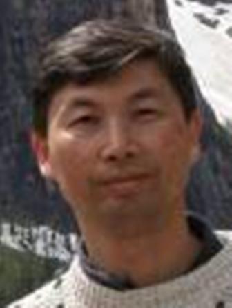
DR. JUNG-SUK GOO
(AMD, Sunnyvale, CA) |
 |
Jung-Suk Goo received his BSEE from Yonsei
University, Seoul, Korea, and MSEE and PhDEE from Stanford University,
CA, in 1997 and 2001 respectively. From 1988 to 1995, he was with
LG Semicon, Korea, working on CMOS technology development for EPROM and
DRAM. During his graduate study, he worked on high-frequency noise
modeling, CMOS low-noise amplifier design, and nano-scale MOSFET
modeling, demonstrating a world-record CMOS low-noise amplifier with
noise figure of 0.9dB. Upon graduation, he joined the Strategic
Technology Group of AMD working on strained silicon and high-K
integration and modeling issues. In 2003, he moved to the Compact
Modeling and Characterization Group where he is currently Senior Member
of Technical Staff. His responsibilities include advanced
characterization and modeling of PD-SOI CMOS, statistical modeling, and
aging (NBTI, HCI) simulation. He holds 25 US patents and has
authored and co-authored over 50 international journal and conference
papers on compact modeling, CMOS RF circuits, CMOS technology, TCAD, and
reliability issues. |
|
|
|
|