|
 |
|
|

Technical
Seminars (Double-Feature) |
|
|
|
|
|
Seminar 1: A 45nm
SOI-CMOS Dual-PLL Processor Clock System for Multi-Protocol I/O |
|
|
Seminar 2: An Embedded
All-Digital Circuit to Measure PLL Response |
|
|
DATE/TIME
Friday, March 25, 2011 (9:00am to 10:30am) |
|
PLACE
AMD Fort Collins Campus (Fort
Collins, CO)
|
|
DIRECTIONS
|
|
From I-25, take Harmony Road Exit (Exit 265) westbound, and enter AMD
campus on right immediately following Harmony/Ziegler intersection.
AMD is located on the NW corner of Harmony Road and Ziegler Road.
Proceed to 3rd floor for escort to seminar auditorium. Non-AMD
employees: please arrive at 8:45am for security sign-in and escort. |
|
COST
Free. As always, food &
drinks will be provided. |
|
RSVP
Send e-mail to
steven.martin@avagotech.com. |
|
|
SEMINAR 1 ABSTRACT (A 45nm SOI-CMOS Dual-PLL
Processor Clock System for Multi-Protocol I/O) |
|
This presentation
will be an encore of a ISSCC 2010 presentation.
A dual-PLL system for 45nm SOI-CMOS
processors is designed to clock a multi-protocol wireline I/O for
high-speed digital communication, covering a frequency range from 1GHz
up to 11.1GHz. The two PLLs, based on a ring and LC-tank VCO, achieve
0.99ps and 0.55ps rms jitter respectively. Circuit and architectural
techniques to minimize the impact of SOI floating-body effect on phase
jitter have been introduced. |
|
|
SEMINAR 2 ABSTRACT (An Embedded All-Digital
Circuit to Measure PLL Response) |
|
This presentation will be an encore of a CICC
2009 presentation. We present an all-digital measurement circuit that
enables wafer-level test and characterization of phase-locked loop (PLL)
response. Through modifications only in the PLL feedback divider state
machine, this technique facilitates accurate estimation of PLL
frequency-domain closed-loop bandwidth and gain peaking by respectively
measuring the time-domain crossover time and maximum overshoot of phase
error to a self-induced phase step in the feedback clock. These
transient measurements are related back to bandwidth and peaking through
the proportionality relationships of crossover time to reciprocal
bandwidth and maximum overshoot to peaking. The design-for-test circuit
can be used to generate a transient plot of step response, measure
static phase error, and observe phase-lock status.We report silicon
results from two demonstration vehicles built in a 45-nm SOI-CMOS logic
technology for high-performance microprocessors. |
|
|
PRESENTATION SLIDES
Seminar 1 pdf
Seminar 2 pdf |
|
|
REFERENCES
(copyright by IEEE) |
- D. Fischette, A. Loke, M. Oshima, B.
Doyle, R. Bakalski, R. DeSantis, A. Thiruvengadam, C. Wang, G. Talbot,
E. Fang, "A 45nm SOI-CMOS
dual-PLL processor clock system for multi-protocol I/O," in IEEE
Int. Solid-State Circuits Conf. Tech. Dig. (San Francisco, CA), pp.
246-247, Feb. 2010.
- D. Fischette, R. DeSantis, and J. Lee, "An
on-chip all-digital measurement circuit ro characterize phase-locked
loop response in 45-nm SOI," in Proc. IEEE Custom Integrated
Circuits Conf. (San Jose, CA), pp. 609-612, Sep. 2009.
- D. Fischette, A. Loke, R. DeSantis, and
G. Talbot, "An embedded
all-digital circuit to measure PLL response," IEEE J. Solid-State
Circuits, vol. 45, no. 8, pp. 1492-1503, Aug. 2010.
|
|
|
DENNIS
FISCHETTE (AMD, Sunnyvale, CA)
|
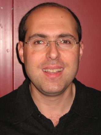 |
Dennis M. Fischette (M’95) received the BS
degree in applied and engineering physics in 1986 from Cornell
University, Ithaca, NY, and studied the History of Science at the
University of California, Berkeley,
from 1986 to 1988. He is a Principal Member of Technical Staff at
Advanced Micro Devices (AMD), Sunnyvale, CA. His technical interests
include PLL and high-speed I/O design and circuit analysis software.
Before joining AMD, he worked for Integrated CMOS
Systems, HaL Computer Systems, and Chromatic Research as a custom
circuit designer (analog, digital, and memory) and CAD software
developer. He is the author of three technical publications and has
taught invited short courses at ISSCC and Symposia on VLSI Technology
and Circuits. Mr. Fischette is a former IEEE Solid-State Circuits
Society Distinguished Lecturer and ISSCC technical committee member and
currently serves as a CICC technical program committee member. |
|
|
|
|
|
|
|