|
 |
 |
|

Technical
Seminars |
 |
 |
|
|
|
Seminar #1: A Versatile Low-Jitter PLL in 90nm CMOS for
SerDes Transmitter Clocking |
|
Seminar #2: IJTAG
(Internal JTAG): A Step Toward a DFT Standard |
|
|
DATE/TIME
Thursday, September 15, 2005 (4:30pm to 6:00pm) |
|
PLACE
Bldg. 1 Auditorium (Agilent Technologies,
Fort Collins, CO) |
|
DIRECTIONS
From I-25, take Harmony Road Exit (Exit 265)
westbound, and enter Agilent/HP campus on right. Agilent/HP campus
is on the NE corner of Harmony Road and Ziegler Road. Proceed to
Bldg. 1 Lobby to sign-in and meet host for escort to Auditorium. |
|
Non-Agilent
Attendees: Please arrive punctually at 4:15pm as you will need to be
escorted to the seminar room. We appreciate a courtesy RSVP to
bob_barnes@agilent.com to
expedite sign-in and to help us with a headcount estimate for
food/drinks. |
|
COST
Free. As always, pizza &
drinks will be provided. |
|
|
SEMINAR #1 |
|
A Versatile Low-Jitter PLL in 90nm CMOS for
SerDes Transmitter Clocking |
|
ABSTRACT
A low-jitter charge-pump PLL is built in
90-nm CMOS for 1-10 Gb/s SerDes transmitter clocking. The PLL
employs a programmable dual-path loop filter with integrating path and
novel resistorless proportional path that can be independently
controlled and accurately modeled for flexible setting of closed-loop
bandwidth and peaking. Frequency is synthesized using an
area-efficient LC-VCO with helical inductors and inversion-mode nFET
varactors for 45% tuning range. The PLL exhibits 0.81 ps rms
jitter at 10 Gb/s. Technology considerations for improving design
manufacturability, tuning range, and jitter performance are addressed. |
|
AUTHORS
Alvin Loke, Bob Barnes, Tin Tin Wee, Mike Oshima, Charles Moore, Ron
Kennedy, Jim Barnes, Bob Zimmer, Kari Arave, Herman Pang, Tom Cynkar,
Aaron Volz, Jim Pfiester, Rob Martin, Bob Miller, David Hood, Gordon
Motley, Ed Rojas, Tom Walley, and Mike Gilsdorf (Agilent Technologies) |
|
REFERENCES |
- A. Loke et al., "A Versatile
Low-Jitter PLL in 90-nm CMOS for SerDes Transmitter Clocking," Proc.
IEEE Custom Integrated Circuits Conf., Sep. 2005.
paper
presentation
(copyright by IEEE)
- A. Loke et al., "A Versatile
90-nm CMOS Charge-Pump PLL for SerDes Transmitter Clocking," IEEE J.
Solid-State Circuits, vol. 41, no. 8, pp. 1894-1907, Aug. 2006.
extended paper
(copyright by IEEE)
|
|
BIOGRAPHY OF SPEAKER |
|
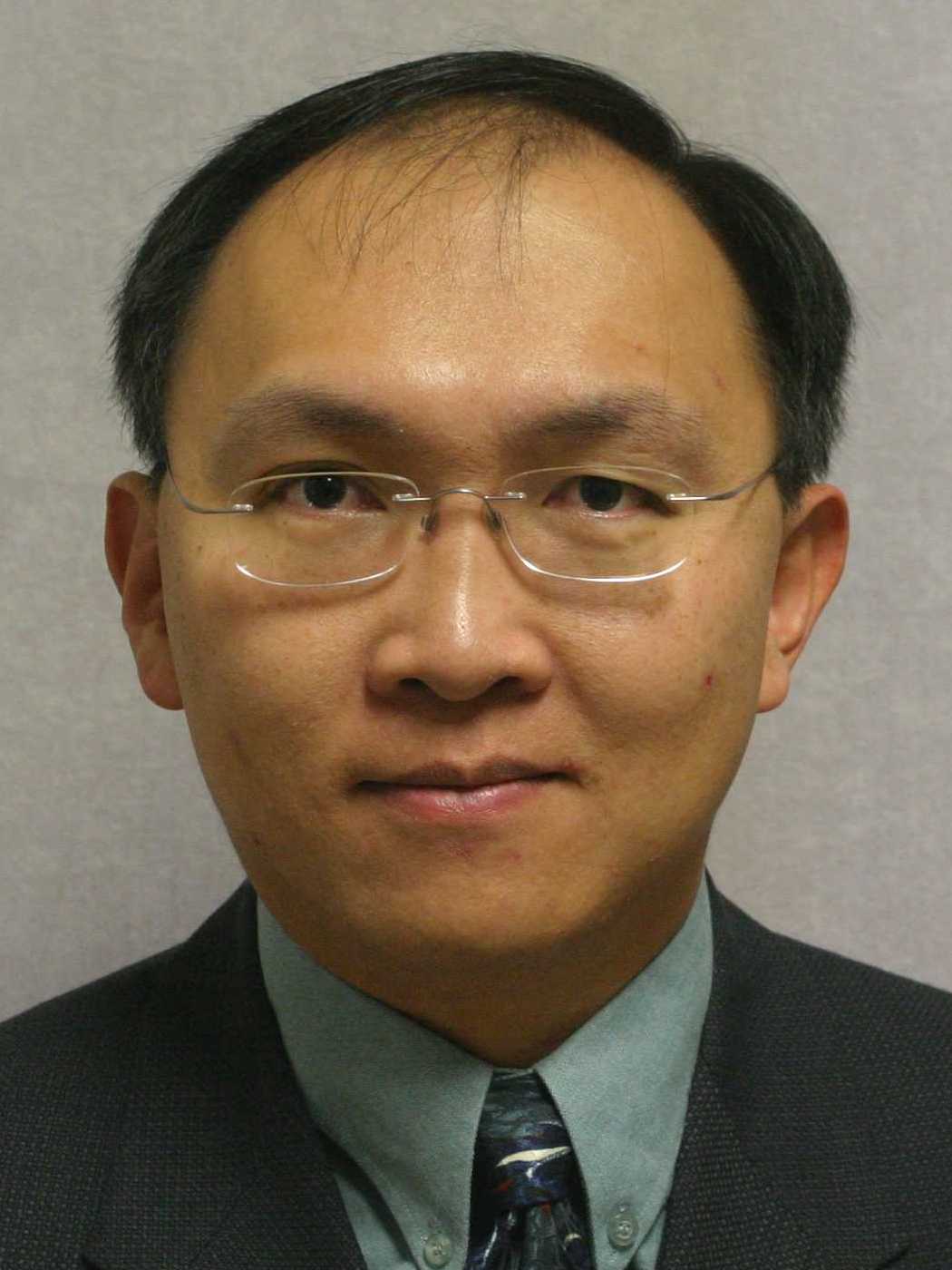
DR. ALVIN LOKE
(Agilent
Technologies, Fort Collins, CO)
|

|
Alvin Loke received his BASc (Eng. Physics) degree with highest honors from the University of British Columbia,
Vancouver, Canada, in 1992, and the MSEE and PhDEE degrees from Stanford University, Stanford, CA, in 1994 and
1999 respectively. He was recipient of the Canadian NSERC 1967 Graduate
Scholarship. While at Stanford, his research focused on
interconnect process integration issues with copper and low-K polymer
dielectrics. He has also served as teaching assistant in
graduate-level device physics courses. Dr. Loke is author/co-author in over 20 technical
publications, and one patent with several pending. He held internships at Texas
Instruments ( Dallas, TX), Motorola (Austin, TX), and at Sumitomo
Electric Industries (Osaka, Japan). In 1998, he joined Hewlett-Packard Laboratories,
Palo Alto, CA where he was involved in process integration of deep
submicron ferroelectric memory for embedded applications. |
|
In
1999, when Agilent Technologies was spun off from Hewlett-Packard, he took a
two-year assignment in Chartered Silicon Partners, Singapore, as Senior
Process Integration Engineer engaged in copper and local interconnect module integration. In 2001, he
transferred to Fort Collins, CO
where he is presently Design Engineer developing 90nm CMOS mixed-signal phase-locked
loop circuits for embedded SerDes I/O and ASIC core clocking applications. |
|
|
SEMINAR #2 |
|
IJTAG (Internal JTAG): A Step Toward a DFT Standard |
|
ABSTRACT
The widespread use of the IEEE 1149.1
Standard Test Access Port as the interface for not only boundary scan
but also for access to device-internal test features has led to a highly
useful but highly fragmented opportunity for the test community.
The need for a standard description of internal test features and
protocols is elucidated, and the framework for the extension of the
Boundary Scan Standards as launched by the ad hoc IJTAG working
group is described. |
|
AUTHORS
Jeff Rearick (Agilent Technologies), Bill Eklow (Cisco Systems), Ken
Posse (Independent Consultant), Al Crouch (Inovys), and Ben Bennetts (Bennetts
Associates) |
|
REFERENCE
Presentation Slides
(copyright by IEEE) |
|
BIOGRAPHY OF SPEAKER |
|
JEFF
REARICK (Agilent
Technologies, Fort Collins, CO) |
 |
Jeff Rearick joined Hewlett Packard in 1984
after earning his BSEE from Purdue University, Lafayette, IN. His
early work on generating manufacturing tests for large digital chips led
him toward the R&D lab and into the CAD tools group to work on design
and test automation software. During this time, Mr. Rearick received
an HP Fellowship to attend the University of Illinois, Urbana-Champaign,
IL, at which he earned his MSEE in 1993. He returned to continue his
test work by focusing on Design-For-Test methodologies and circuits for HP
Precision Architecture processors and support chips, for which he has
earned over 20 patents and many publications. Since being spun-off
from HP into Agilent Technologies, Mr. Rearick has continued his test work
on large high-performance ASICs, leading to recent work on high-speed I/O
testing (some of which became IEEE Stardard 1149.6, for which he served on
the working group) as well as embedded analog instrumentation. |
|
|