|
 |
|
|

Technical
Seminar |
|
|
|
|
|
Introduction to Deep Submicron CMOS Device
Technology and Its Impact on Circuit Design
|
|
|
DATE/TIME
Wednesday, December 8, 2004 (5:00pm to 6:30pm)
|
|
PLACE
|
- Physiology Bldg. Room 103 (1st floor) (CSU, Fort Collins, CO)
- Same room as November 2004 meeting (Dr.
Don Morris' seminar)
|
|
DIRECTIONS
|
-
To
Colorado State University
-
To
Physiology Building Room 103
-
Physiology
Building is on the south side of campus, at the NE corner of Centre
Avenue and Lake Street. From I-25, it is easiest to take
Prospect Road westbound. After passing College Avenue, turn
right onto Centre Avenue and park at parking lot on right side of road
before reaching Lake Street.
-
Park south of
Physiology Building -- free after 4pm
|
|
COST
Free. As always, pizza &
drinks will be provided. |
|
|
ABSTRACT In
the past decade, global demand for higher speed,
higher density, lower cost, and more reliable silicon IC's has led to
the continuous scaling of CMOS technologies into the very deep submicron
realm. With increasing integration and reliability difficulties
introducing very low-K dielectrics in the copper interconnect backend, the need
to accelerate the scaling of CMOS devices in the frontend has become more
critical in achieving performance benchmarks. This tutorial presents
basic device design challenges in deep submicron CMOS technologies and
explains how these difficulties motivate additional complexities in
transistor fabrication from isolation to silicidation modules.
Topics include reverse short- and narrow-channel effects, subthreshold
conduction, gate leakage, multiple-VT devices, shallow trench isolation, source/drain and well
engineering, and self-aligned silicidation to name a few. The goal
of this tutorial is to provide an intuitive (non-mathematical) understanding of device physics and fabrication concepts in deep submicron
CMOS so as to better evaluate circuit behavior and design tradeoffs. |
|
PRESENTATION SLIDES
pdf |
|
REFERENCES (most
recent first)
|
- T. B. Hook et
al., �Lateral Ion Implant Straggle and Mask Proximity Effect,�
IEEE Trans. Electron Devices, vol. 50, no. 9, pp. 1946-1951,
Sept. 2003.
- J.
Assenmacher, �BSIM4 Modeling and Parameter Extraction,� Technical
Univ. Berlin Analog Integrated Circuits Workshop, Mar. 2003.
- X.
Xi et al., BSIM4.3.0 MOSFET Model � User�s Manual, The
Regents of the University of California at Berkeley, 2003.
- International
Technology Roadmap for Semiconductors, Front End Processes
(2003 Edition), 2003.
- H.-S. P.
Wong, �Beyond the Conventional Transistor,� IBM Journal of
Research & Development, vol. 46, no. 2/3, pp. 133-168, Mar.
2002.
- Y. Taur,
�CMOS Design Near the Limit of Scaling,� IBM Journal of
Research & Development, vol. 46, no. 2/3, pp. 213-222, Mar.
2002.
- C. R.
Cleavelin, �Front End Manufacturing Technology,� IEEE IEDM
Short Course on The Future of Semiconductor Manufacturing, Dec.
2002.
- D.
Harame, �RF Device Technologies,� IEEE IEDM Short Course on RF
Circuit Design for Communication Systems, Dec. 2002.
- S.
Thompson et al., �A 90nm Logic Technology Featuring 50nm
Strained Silicon Channel Transistors, 7 Levels of Cu Interconnect, Low
k ILD, and 1�m2 SRAM
Cell,� IEEE IEDM Tech. Digest, pp. 61-64, Dec. 2002.
- C. C. Wu et
al., �A 90nm CMOS Device Technology with High-Speed ,
General-Purpose, and Low-Leakage Transistors for System on Chip
Applications,� IEEE IEDM Tech. Digest, pp. 65-68, Dec. 2002.
- R. Rios et
al., �A Three-Transistor Threshold Voltage Model for Halo
Processes,� IEEE IEDM Tech. Digest, pp. 113-116, Dec. 2002.
- R.A.
Bianchi et al., �Accurate Modeling of Trench Isolation
Induced Mechanical Stress Effects on MOSFET Electrical Performance,�
IEEE IEDM Tech. Digest, pp. 117-120, Dec. 2002.
- B. Razavi, Design of Analog CMOS Integrated
Circuits, McGraw-Hill, 2001.
- J. D. Plummer et al., Silicon VLSI
Technology� Fundamentals, Practice and Modeling, Prentice-Hall,
2000.
- K. M. Cao et
al., �Modeling of Pocket Implanted MOSFETs for Anomalous Analog
Behavior,� IEEE IEDM Tech. Digest, pp. 171-120, Dec. 1999.
- A.
Chatterjee et al., �Transistor Design Issues in Integrating
Analog Functions with High Performance Digital CMOS,� IEEE Symp.
VLSI Technology Tech. Digest, pp. 147-148, June 1999.
- T. H. Lee, The Design of CMOS Radio-Frequency
Integrated Circuits, Cambridge University Press, 1998.
- D. P. Foty, MOSFET Modeling with SPICE:
Principles and Practice, Prentice-Hall, 1996.
- A. Beiser, Concepts in modern Physics (4th ed.), McGraw-Hill, 1987.
- S.M. Sze, Physics of Semiconductor Devices (2nd ed.), John Wiley &
Sons, 1981.
|
|
|
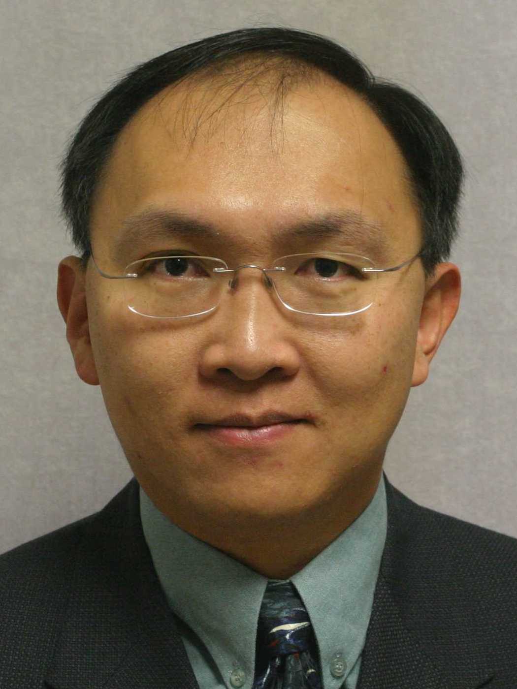
DR, ALVIN LOKE
(Agilent
Technologies, Fort Collins, CO)
|
|
Alvin Loke received his BASc (Eng. Physics) degree with highest honors from the University of British Columbia,
Vancouver, Canada, in 1992, and the MSEE and PhDEE degrees from Stanford University, Stanford, CA, in 1994 and
1999 respectively. He was recipient of the Canadian NSERC 1967 Graduate
Scholarship. While at Stanford, his research focused on
interconnect process integration issues with copper and low-K polymer
dielectrics. He has also served as teaching assistant in
graduate-level device physics courses. Dr. Loke is author/co-author in over 20 technical
publications, and one patent with several pending. He held internships at Texas
Instruments ( Dallas, TX), Motorola (Austin, TX), and at Sumitomo
Electric Industries (Osaka, Japan). In 1998, he joined Hewlett-Packard Laboratories,
Palo Alto, CA where he was involved in process integration of deep
submicron ferroelectric memory for embedded applications. |
|
In
1999, when Agilent Technologies was spun off from Hewlett-Packard, he took a
two-year assignment in Chartered Silicon Partners, Singapore, as Senior
Process Integration Engineer engaged in copper and local interconnect module integration. In 2001, he
transferred to Fort Collins, CO
where he is presently Design Engineer developing 90nm CMOS mixed-signal phase-locked
loop circuits for embedded SerDes I/O and ASIC core clocking applications. |
|
|
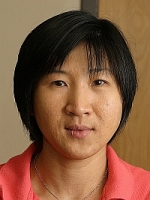
TIN TIN WEE
(Agilent
Technologies, Fort Collins, CO)
|
|
Tin Tin Wee received her BTech (Electronics Eng.)
from the National University of Singapore, Singapore, in 1999. Prior
to receiving her BTech, she was an Associate Engineer at International
Video Products, Singapore, where she involved in RF test, measurement, and
failure analysis of consumer video electronics. In 1996, she joined Chartered Semiconductor
Manufacturing, Singapore, as Process Integration Engineer where she was
engaged in multiple aspects of 0.25um, 0.18um, and 0.15um technology
development and transfer. Activities included SRAM development,
yield enhancement, and most recently, copper and local interconnect module
integration. Ms. Wee returned to the National University of
Singapore to study circuits and systems, and completed her MSEE degree
in 2001. |
|
She now resides in Fort Collins, CO, as Design Engineer at Agilent
Technologies where she is involved in bench test, characterization, and
debug of 130nm and 90nm CMOS ASIC's with embedded SerDes and core clocking
PLL's. She hold two patents. |
|
|
DR, JIM PFIESTER (Agilent
Technologies, Fort Collins, CO)
|

|
Jim Pfiester received his BSEE (summa
cum laude) and MSEE degrees from the University of Illinois,
Urbana-Champaign, IL, in 1976 and 1977 respectively. He received his PhDEE degree from Stanford University, Stanford, CA, in 1984. His
dissertation investigated the performance limits of CMOS VLSI. From
1978 to 1980, he was employed by Motorola, Inc., Austin, TX, as a Circuit
Designer on the MC68000 16-b microprocessor chip. From 1981 to 1983, he
was a Device Physics Consultant for Hewlett-Packard. From 1984 to 1985, he
was a Research Staff Member at the IBM Thomas J. Watson Research Center,
Yorktown Heights, NY, and was involved in the design of submicrometer CMOS
devices.
|
|
From 1985 to 1995, he was Member of Technical Staff at Motorola's
Advanced Products Research and Development Laboratory, Austin, TX, where
he was involved in the development of advanced CMOS technologies. In 1995, Dr. Pfiester joined the
Hewlett-Packard Company, later becoming Agilent Technologies, in Fort
Collins, CO. |
|