rtsd

The 23rd International Symposium on Room-Temperature Semiconductor Detectors (RTSD) represents the largest forum of scientists and engineers developing improved semiconductor radiation detectors and imaging arrays. Room-temperature solid-state radiation detectors for X-ray, gamma-ray, and neutron radiation are increasingly finding applications in several diverse fields, such as medicine, homeland security, astrophysics and environmental remediation. The objective of this workshop is to provide a forum for discussion of the state of the art in the development of photoconductive materials for radiation detection, material and detector characterization, device fabrication processes, electronics and applications. Oral and poster presentations representing a broad spectrum of research activities emphasizing either device or material understanding are sought.

Authors are encouraged to submit abstracts on original work in the areas listed below.


Ralph James
RTSD Program Co-Chair
Brookhaven National Laboratory, USA

Michael Fiederle
RTSD Program Co-Chair
University of Freiburg, Germany
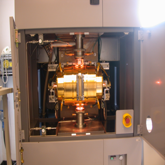
The performance of room-temperature semiconductor radiation detectors is inextricably linked to the quality of the crystals used to fabricate the detectors. Consequently, the identification and resolution of the remaining material problems is a critical element to further the deployment of the technology. Remarkable progress has occurred to understand the roles of Te-rich inclusions/precipitates, dislocations and sub-grain boundaries on CZT device response. This knowledge has shaped the R&D efforts at many institutions. Despite this progress, three major material issues remain that limit the use of the detector technology: (1) non-uniformity in the material created by extended defects, (2) carrier trapping due to point defects, and (3) the relatively high cost of large-volume gamma-ray spectrometers with energy resolutions less than 1% at 662 keV. To address these problems further investigations are needed to correlate the material, device properties, and growth processes, so that the results can be effectively applied toward timely improvements in crystal growth and processing strategies.

Three-dimensional position sensitive gamma-ray spectrometers have been constructed and tested. Each pixel location provides the interaction's lateral coordinates, while the cathode/anode signal ratio and the electron drift time are both used to obtain the interaction depth. Data-acquisition and processing software have been developed to perform calibration and real-time spectroscopy and reconstruct images of radiation sources around the detector. This session focuses on 3D detectors produced from CZT and other semiconductors, improvements in spectroscopic performance and position sensing, charge sharing, ASIC readout, image reconstruction, system integration and applications.

Multi-pixel, strip, virtual Frisch-grid, co-planar grid detectors and other electrode configurations serve as the principal method to make high-resolution gamma-ray spectrometers, since the signal used to obtain the pulse-height spectrum is dominated by the transport of electrons, and the hole transport can be mostly ignored. Some of these device designs are also critical for imaging systems, since they convey positional information when used in conjunction with a collimator or coded aperture mask, or when used as a Compton imager. Data based on these electrode designs, as well as new electrode layouts, will be included in sessions devoted to this subject.

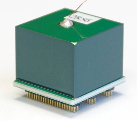
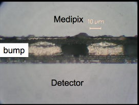
The hybridization, interconnects and related read-out electronics play an important role for the development of pixel detectors. Novel approaches are required to use the potential of the Room Temperature Semiconductors Detectors for the production and application of pixel detectors.

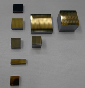
Semiconductor for radiation detection cover a wide range of materials. This symposium is a platform for the discussion of established materials like CdTe, CZT and GaAs, as well as for novel materials. Experimental and theoretical approaches are welcome to discuss advances in the development of semiconductor materials.

In the recent years several papers have been published of radiation detectors based on organic materials. In this session an overview will be given, and the latest results on the development of these detectors will be presented by other contributors for this innovative class of materials.

Radiation detectors are electrical devices and require electrical contacts. The behavior of metal/semiconductor contacts and their characteristics often control the performance. The fabrication and the characterization of contacts are part of this session.

Detectors based on compound semiconductors can potentially change under voltage bias, or due to exposure to a high flux of incident radiation – a phenomenon generally referred to as “polarization”. The polarization is often due to the buildup of space charge in the detectors from hole trapping or by contact contributions. In most cases the internal electric field distribution is affected and changes as a function of time and other parameters. This session will focus on an understanding of polarization behavior affecting carrier transport and ways to mitigate the adverse consequences. Other factors affecting long-term detector stability, such as exposure to air, aging, and damage from particle bombardment, will also be included in this session.

The combination of scintillator and semiconductor are promising concepts for hybrid detector systems. The focus of this session is dedicated to the integration of Room Temperature Semiconductor Detectors and other related technology issues.

Solid-state neutron detectors have many potential advantages over other approaches. This session focuses on micro-structured semiconductor neutron detectors, thin-film detectors, and materials for direct conversion of neutrons to electron-hole pairs. Modeling, material development, fabrication, materials/device characterization, prototype instruments and applications will be included.

This session will emphasize technologies to improve capabilities to detect, localize, characterize, or safeguard nuclear and radiological materials for security, non-proliferation and forensics applications. Most abstracts will emphasize potential improvements in performance, cost, or operational burden of the detection approach. A wide spectrum of abstracts is encouraged, dealing with basic and applied research, engineering development, and/or systems evaluation.

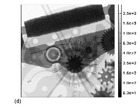
Multiple sessions are planned to cover the applications of position-sensitive, room-temperature semiconductor radiation detectors for medical, space, baggage scanning, and other non-destructive imaging of objects. Many of the applications will take advantage of the compact design and energy resolution offered by semiconductors. The imaging sessions will focus on one or more of the following areas: (1) the development of position-sensitive detector modules, (2) the integration of detectors into prototypical instruments, and (3) the use and testing of the instruments in the lab and field. All room-temperature-operating semiconductors detectors, such as CdTe, CZT, Si, GaAs, and neutron-absorbing materials, will be considered. New developments pertaining to the electronic chips used for readout of multi-pixel and other position-sensing semiconductor detectors and the processes used for bonding assemblies will also be included.